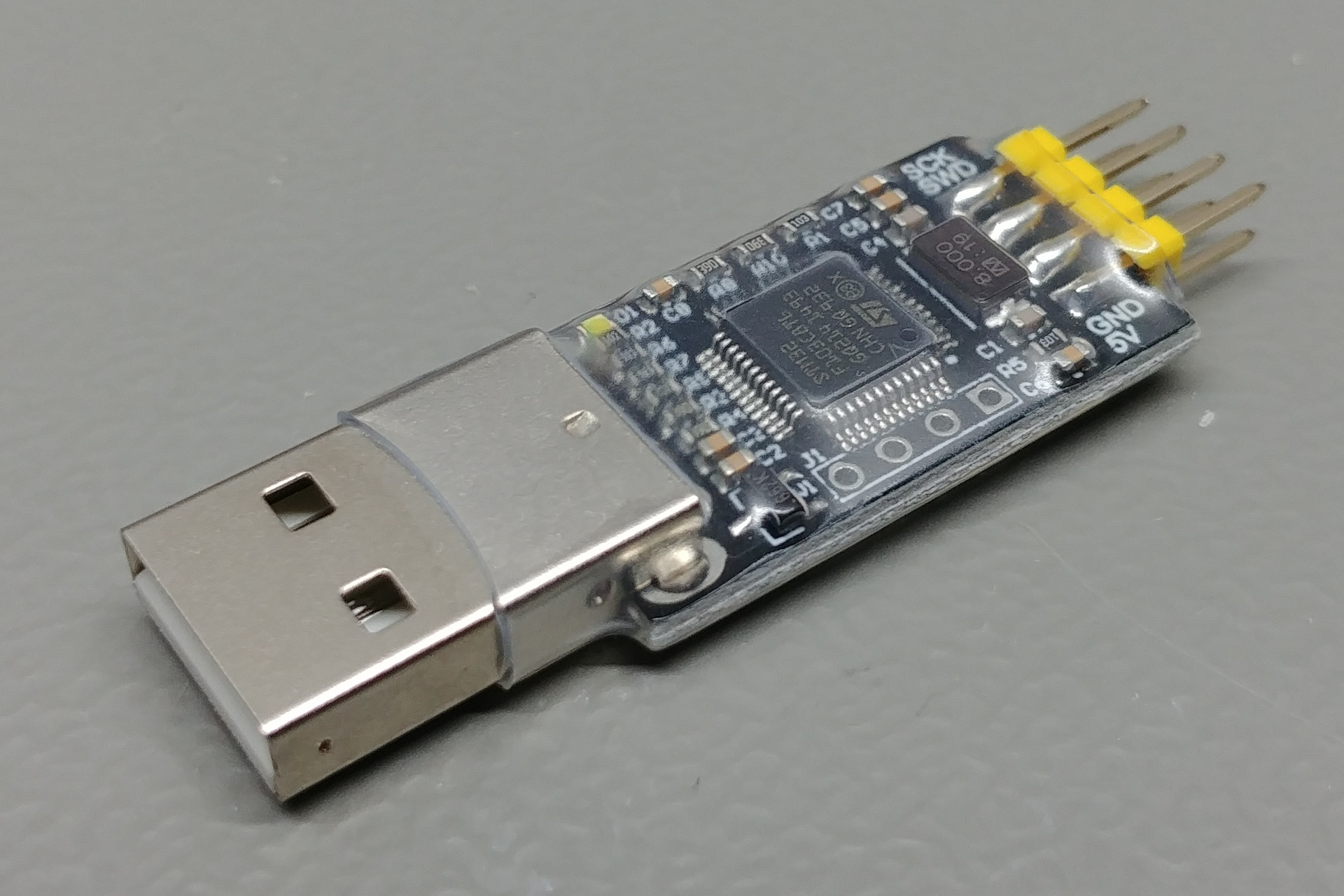
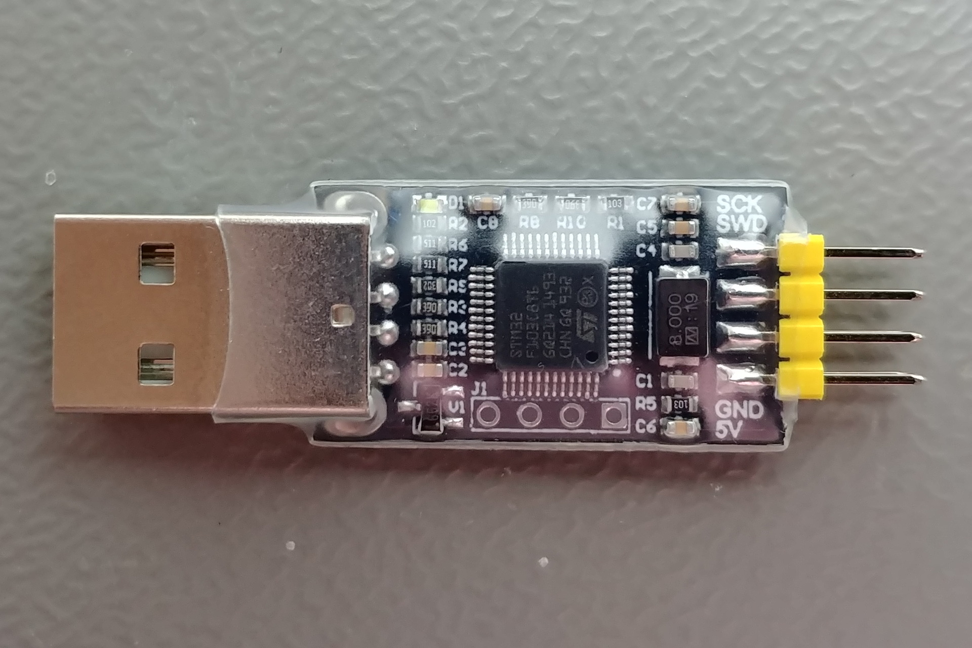
Bare ST-LINK V2 Debugger
STM32F103C8T6
Board
| Name | Bare ST-LINK V2 Debugger |
| Part | Unknown |
| Brand | Unknown |
| Origin | China |
Microcontroller
| Part | STM32F103C8T6 |
| Manufacturer | ST-Microelectronics |
| Core | Arm Cortex-M3 |
| Max. Clock Speed | 72MHz |
| Package | LQFP 48 pins |
Internal memories
| FLASH | 64KiB |
| SRAM | 20KiB |
Oscillators
| HSI | 8MHz |
| LSI | 40kHz |
| HSE | 8MHz |
| LSE | None |
Power
| Sources | USB connector (+5V) |
| VDDA pin | No |
| VSSA pin | No |
| VREF- pin | No |
| VREF+ pin | No |
| Backup battery | None |
Regulator
| Manufacturer | Torex Semiconductor LTD. |
| Part | XC6206 (662K) |
| Package | SOT23 3 pins |
| Input | +3.6V to +6V |
| Output | +3.3V @ 200mA |
| Datasheet | XC6206.pdf |
PCB
| Color | Blakc |
| Size (w x l) | 16mm x 28mm |
| Mounting | None |
Remarks
- Note: This board is intended to use as ST-Link device to program and debug other STM32 and STM8 devices.
Pictures
Resources
Inputs & outputs
Activity LED
| Name | - |
| Reference | D1 |
| Type | LED |
| Connected to | PA10 |
| Mode | Source |
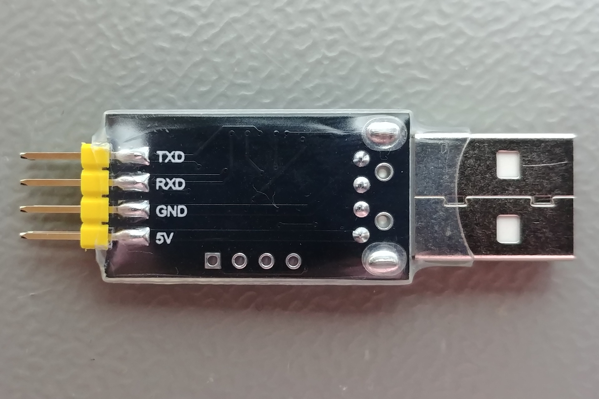
Connectors & headers
SWD out properties
| Name | Unknown |
| Reference | None |
| Type | Pin header (2.54mm, 4x2, male) |
SWD out pins
| # | Name | Function | Connected to |
|---|---|---|---|
| 1 | SCK | - | PA5 |
| 2 | TXD | - | PA9 |
| 3 | SWD | - | PB12 |
| 4 | RXD | - | PA10 |
| 5 | GND | - | Ground plane |
| 6 | GND | - | Ground plane |
| 7 | 5V | - | +5V rail |
| 8 | 5V | - | +5V rail |
SWD in properties footprint
| Name | Unknown |
| Reference | None |
| Type | Pin header (1mm, 4x1, male) |
SWD in pins footprint
| # | Name | Function | Connected to |
|---|---|---|---|
| 1 | - | VCC | +3.3V rail |
| 2 | - | GND | Ground plane |
| 3 | - | SWCLK | PA14 |
| 4 | - | SWDIO | PA13 |
USB A connector properties
| Name | Unknown |
| Reference | None |
| Type | USB A |
USB A connector pins
| # | Name | Function | Connected to |
|---|---|---|---|
| 1 | - | VCC | +5V rail |
| 2 | - | D- | PA11 |
| 3 | - | D+ | PA12 |
| 4 | - | GND | Ground plane |