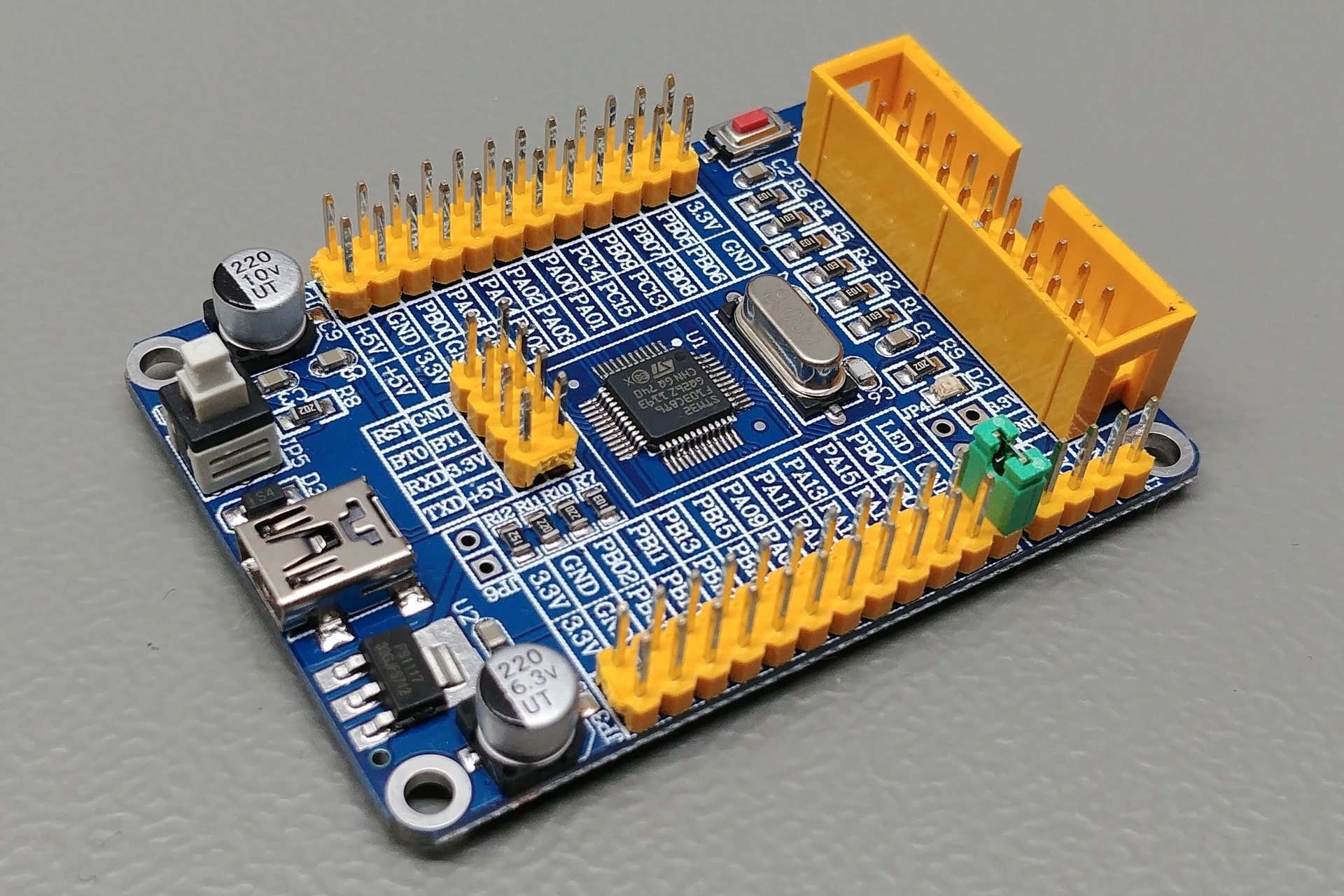
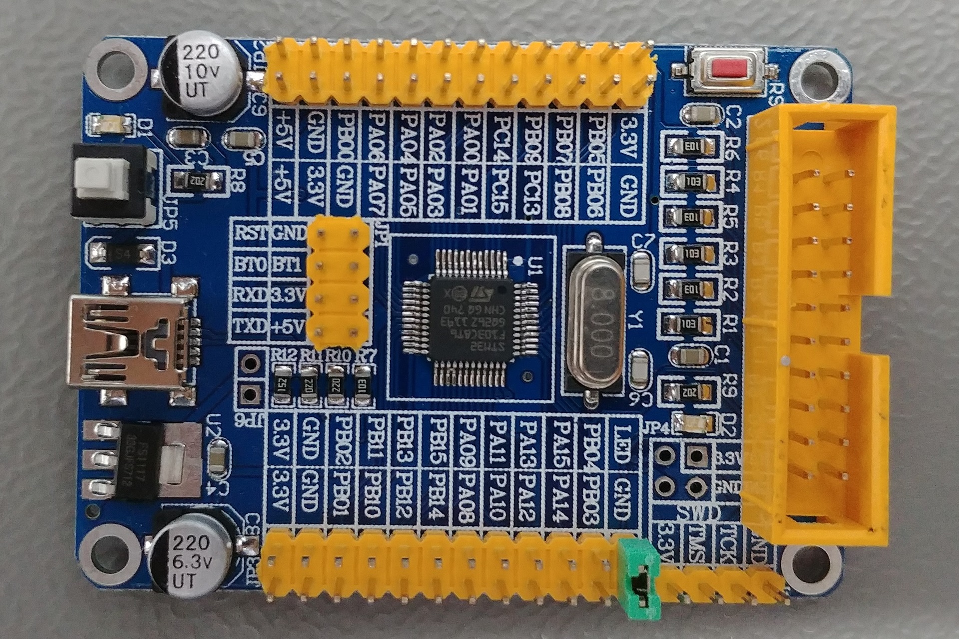
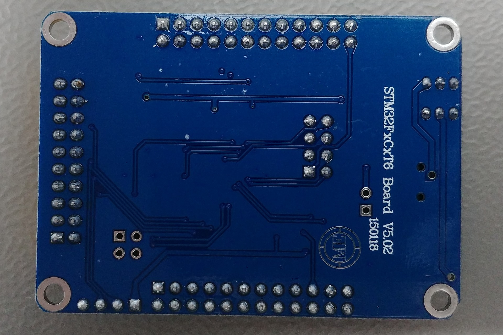
STM32FxCxT6 Board V5.02
STM32F103C8T6
Board
| Name | STM32FxCxT6 Board V5.02 |
| Part | Unknown |
| Brand | Unknown |
| Origin | China |
Microcontroller
| Part | STM32F103C8T6 |
| Manufacturer | ST-Microelectronics |
| Core | Arm Cortex-M3 |
| Max. Clock Speed | 72MHz |
| Package | LQFP 48 pins |
Internal memories
| FLASH | 64KiB |
| SRAM | 20KiB |
Oscillators
| HSI | 8MHz |
| LSI | 40kHz |
| HSE | 8MHz |
| LSE | None |
Power
| Sources | Any +3.3V pin (+3.3V) Any +5V pin (+5V) USB connector (+5V) |
| VDDA pin | No |
| VSSA pin | No |
| VREF- pin | No |
| VREF+ pin | No |
| Backup battery | None |
Regulator
| Manufacturer | Fortune Semiconductor Corp. |
| Part | FS1117 (FS1117) |
| Package | SOT223 3 pins |
| Input | +4.7V to +23V |
| Output | +3.3V @ 1A |
| Datasheet | FS1117.pdf |
PCB
| Color | Blue |
| Size (w x l) | 45mm x 63mm |
| Mounting | 4x mounting hole (M3) |
Remarks
- Warning: The +5V pins on this board are directly connected to the +5V pin of the USB connector. There is no protection in place. Do not power this board through USB and an external power supply at the same time.
Pictures
Resources
Devices
None
Inputs & outputs
Reset button
| Name | RST |
| Reference | - |
| Type | Button |
| Connected to | NRST |
| Mode | Active low |
Power source switch
| Name | - |
| Reference | JP5 |
| Type | Switch |
| Connected to | +5V USB |
| Mode | N.A. |
User LED enable
| Name | - |
| Reference | - |
| Type | 1-way jumper |
| Connected to | User LED |
| Mode | N.A. |
- Note: This jumper is part of Header 2
Power LED
| Name | - |
| Reference | D1 |
| Type | LED |
| Connected to | +3.3V rail |
| Mode | N.A. |
User LED
| Name | - |
| Reference | D2 |
| Type | LED |
| Connected to | PC13 |
| Mode | N.A. |
Connectors & headers
Header 1 properties
| Name | Unknown |
| Reference | JP2 |
| Type | Pin header (2.54mm, 12x2, male) |
Header 1 pins
| # | Name | Function | Connected to |
|---|---|---|---|
| 1 | 3.3V | - | +3.3V rail |
| 2 | GND | - | Ground plane |
| 3 | PB05 | - | PB5 |
| 4 | PB06 | - | PB6 |
| 5 | PB07 | - | PB7 |
| 6 | PB08 | - | PB8 |
| 7 | PB09 | - | PB9 |
| 8 | PC13 | - | PC13 |
| 9 | PC14 | - | PC14 |
| 10 | PC15 | - | PC15 |
| 11 | PA00 | - | PA0 |
| 12 | PA01 | - | PA1 |
| 13 | PA02 | - | PA2 |
| 14 | PA03 | - | PA3 |
| 15 | PA04 | - | PA4 |
| 16 | PA05 | - | PA5 |
| 17 | PA06 | - | PA6 |
| 18 | PA07 | - | PA7 |
| 19 | PB00 | - | PB0 |
| 20 | GND | - | Ground plane |
| 21 | GND | - | Ground plane |
| 22 | 3.3V | - | +3.3V rail |
| 23 | +5V | - | +5V rail |
| 24 | +5V | - | +5V rail |
Header 2 properties
| Name | Unknown |
| Reference | JP3 |
| Type | Pin header (2.54mm, 12x2, male) |
Header 2 pins
| # | Name | Function | Connected to |
|---|---|---|---|
| 1 | LED | - | LED D2 |
| 2 | GND | - | Ground plane |
| 3 | PB04 | - | PB4 |
| 4 | PB03 | - | PB3 |
| 5 | PA15 | - | PA15 |
| 6 | PA14 | - | PA14 |
| 7 | PA13 | - | PA13 |
| 8 | PA12 | - | PA12 |
| 9 | PA11 | - | PA11 |
| 10 | PA10 | - | PA10 |
| 11 | PA09 | - | PA9 |
| 12 | PA08 | - | PA8 |
| 13 | PB15 | - | PB15 |
| 14 | PB14 | - | PB14 |
| 15 | PB13 | - | PB13 |
| 16 | PB12 | - | PB12 |
| 17 | PB11 | - | PB11 |
| 18 | PB10 | - | PB10 |
| 19 | PB02 | - | PB2 |
| 20 | PB01 | - | PB1 |
| 21 | GND | - | Ground plane |
| 22 | GND | - | Ground plane |
| 23 | 3.3V | - | +3.3V rail |
| 24 | 3.3V | - | +3.3V rail |
USB connector properties
| Name | Unknown |
| Reference | None |
| Type | USB Mini |
USB connector pins
| # | Name | Function | Connected to |
|---|---|---|---|
| 1 | - | VCC | +5V rail |
| 2 | - | D- | PA11 |
| 3 | - | D+ | PA12 |
| 4 | - | ID | N.C. |
| 5 | - | GND | Ground plane |
JTAG header properties
| Name | Unknown |
| Reference | None |
| Type | IDC (2.54mm, 10x2, male) |
JTAG header pins
| # | Name | Function | Connected to |
|---|---|---|---|
| 1 | - | VCC | +3.3V rail |
| 2 | - | VCC | +3.3V rail |
| 3 | - | TRST | PB4 |
| 4 | - | GND | Ground plane |
| 5 | - | TDI | PA15 |
| 6 | - | GND | Ground plane |
| 7 | - | TMS / SWDIO | PA13 |
| 8 | - | GND | Ground plane |
| 9 | - | TCLK / SWCLK | PA14 |
| 10 | - | GND | Ground plane |
| 11 | - | RTCK | N.C. |
| 12 | - | GND | Ground plane |
| 13 | - | TDO / SWO | PB3 |
| 14 | - | GND | Ground plane |
| 15 | - | RESET | NRST |
| 16 | - | GND | Ground plane |
| 17 | - | N.C. | N.C. |
| 18 | - | GND | Ground plane |
| 19 | - | N.C. | N.C. |
| 20 | - | GND | Ground plane |
SWD header properties
| Name | SWD |
| Reference | None |
| Type | Pin header (2.54mm, 4x1, male) |
SWD header pins
| # | Name | Function | Connected to |
|---|---|---|---|
| 1 | 3.3V | VCC | +3.3V rail |
| 2 | TMS | SWDIO | PA13 |
| 3 | TCK | SWCLK | PA14 |
| 4 | GND | GND | Ground plane |
Serial and boot header properties
| Name | Unknown |
| Reference | JP1 |
| Type | Pin header (2.54mm, 4x2, male) |
Serial and boot header pins
| # | Name | Function | Connected to |
|---|---|---|---|
| 1 | +5V | - | +5V rail |
| 2 | TXD | - | PA9 |
| 3 | 3.3V | - | +3.3V rail |
| 4 | RXD | - | PA10 |
| 5 | BT1 | - | PB2 |
| 6 | BT0 | - | BOOT0 |
| 7 | GND | - | Ground plane |
| 8 | RST | - | NRST |
Power header properties footprint
| Name | Unknown |
| Reference | JP4 |
| Type | Pin header (2.54mm, 2x2, male) |
Power header pins footprint
| # | Name | Function | Connected to |
|---|---|---|---|
| 1 | 3.3V | - | +3.3V rail |
| 2 | GND | - | Ground plane |
| 3 | 3.3V | - | +3.3V rail |
| 4 | GND | - | Ground plane |