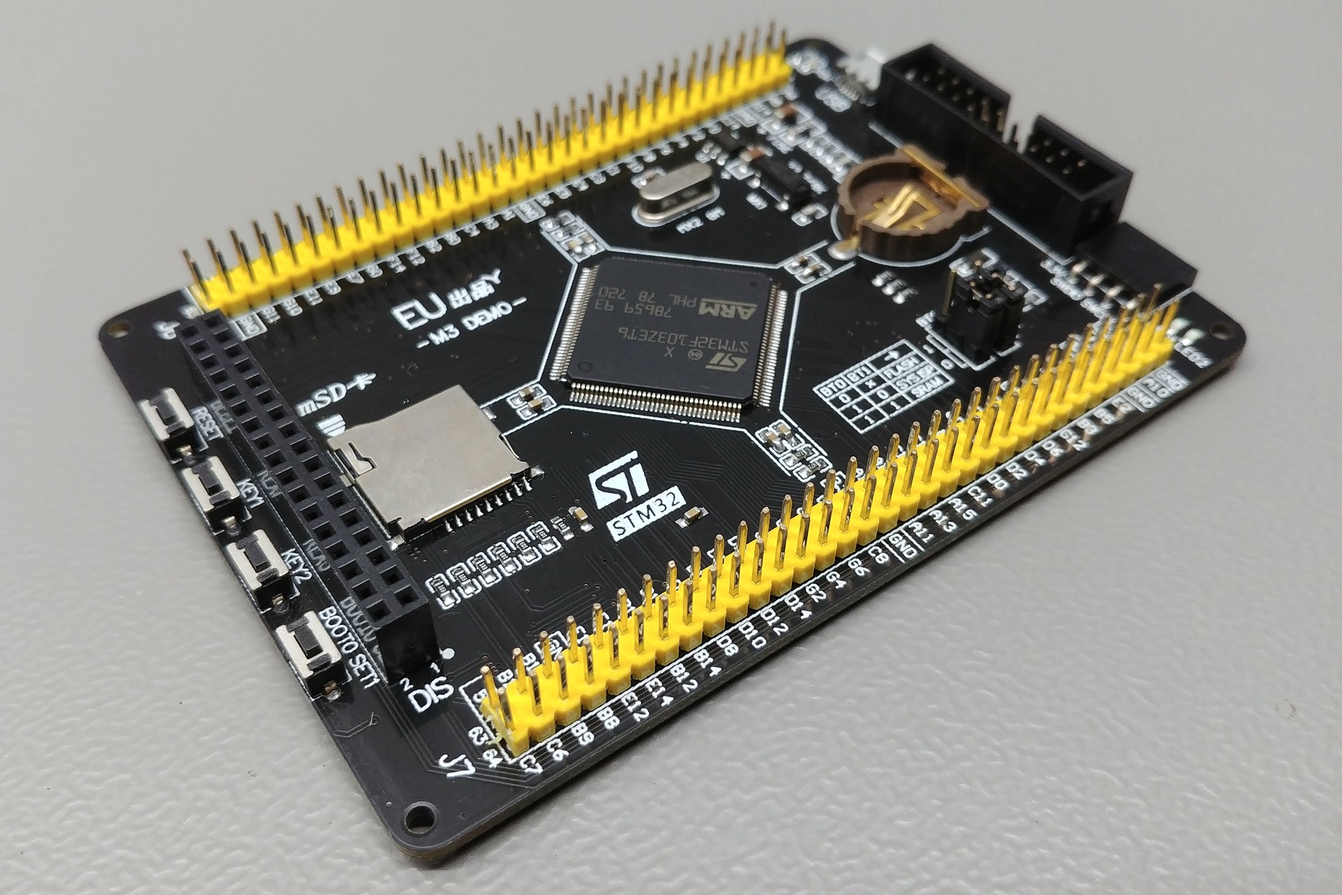
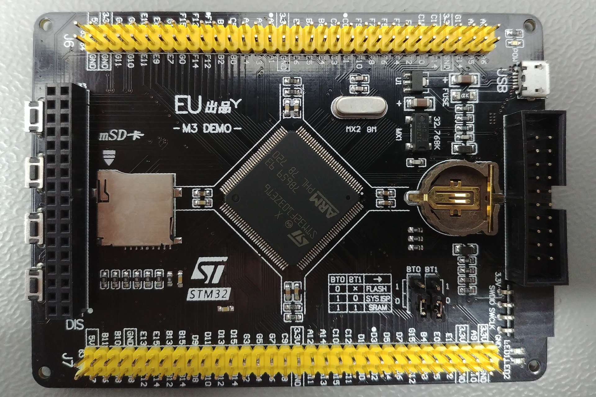
Euse M3 DEMO
STM32F103ZET6
Board
| Name | Euse M3 DEMO |
| Part | Unknown |
| Brand | Euse |
| Origin | China |
Microcontroller
| Part | STM32F103ZET6 |
| Manufacturer | ST-Microelectronics |
| Core | Arm Cortex-M3 |
| Max. Clock Speed | 72MHz |
| Package | LQFP 144 pins |
Internal memories
| FLASH | 512KiB |
| SRAM | 64KiB |
Oscillators
| HSI | 8MHz |
| LSI | 40kHz |
| HSE | 8MHz |
| LSE | 32.768kHz |
Power
| Sources | Any +3.3V pin (+3.3V) Any +5V pin (+5V) USB connector (+5V) |
| VDDA pin | No |
| VSSA pin | No |
| VREF- pin | No |
| VREF+ pin | No |
| Backup battery | Holder (12.5mm / 12) |
Regulator
| Manufacturer | Holtek Semiconductor Inc. |
| Part | HT7833 (HT7833) |
| Package | SOT89-3 3 pins |
| Input | +4.3V to +8.5V |
| Output | +3.3V @ 500mA |
| Datasheet | HT78xx.pdf |
PCB
| Color | Black |
| Size (w x l) | 65mm x 103mm |
| Mounting | 4x mounting hole (M2) |
Remarks
- Warning: The +5V pins on this board are directly connected to the +5V pin of the USB connector. There is no protection in place. Do not power this board through USB and an external power supply at the same time.
Pictures
Resources
Outputs
Devices
Inputs & outputs
Reset button
| Name | RESET |
| Reference | - |
| Type | Button |
| Connected to | NRST |
| Mode | Active low |
BOOT0 jumper
| Name | BT0 |
| Reference | - |
| Type | 2-way jumper |
| Connected to | BOOT0 |
| Mode | N.A. |
BOOT1 jumper
| Name | BT1 |
| Reference | - |
| Type | 2-way jumper |
| Connected to | PB2 |
| Mode | N.A. |
BOOT0 button
| Name | BOOT0 SET1 |
| Reference | - |
| Type | Button |
| Connected to | BOOT0 |
| Mode | Active high |
User button 1
| Name | KEY1 |
| Reference | - |
| Type | Button |
| Connected to | PA0 |
| Mode | Active high |
User button 2
| Name | KEY2 |
| Reference | - |
| Type | Button |
| Connected to | PF11 |
| Mode | Active high |
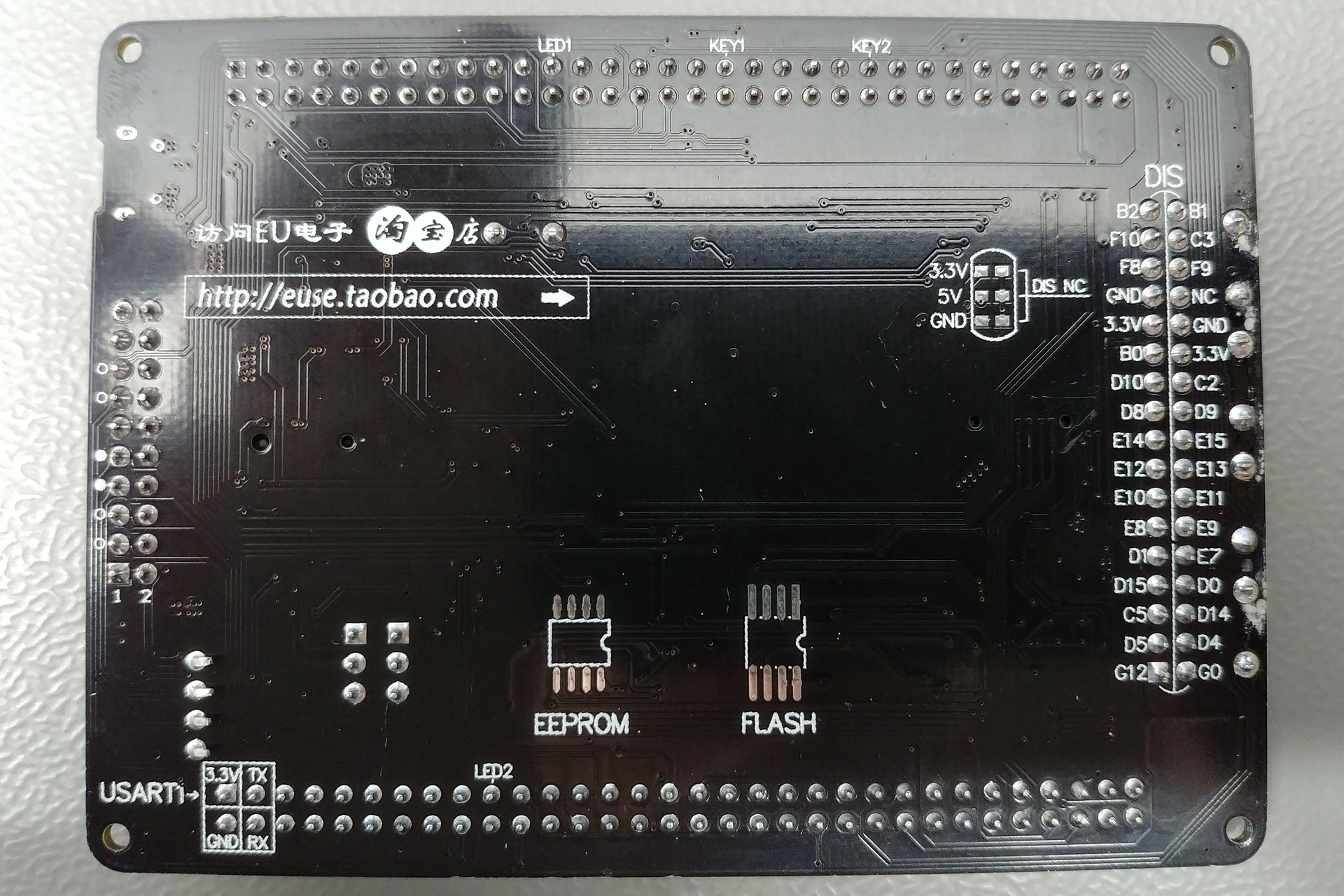
DIS NC solder bridges
| Name | - |
| Reference | - |
| Type | Solder bridge |
| Connected to | Display header NC pin |
| Mode | N.A. |
- Info: Connects the Display NC pin to either +5V, +3.3V or ground.
Power LED
| Name | POW |
| Reference | - |
| Type | LED |
| Connected to | +3.3V rail |
| Mode | N.A. |
User LED 1
| Name | LED1 |
| Reference | - |
| Type | LED |
| Connected to | PC0 |
| Mode | Sink |
User LED 2
| Name | LED2 |
| Reference | - |
| Type | LED |
| Connected to | PD3 |
| Mode | Sink |
Connectors & headers
Header 1 properties
| Name | Unknown |
| Reference | J7 |
| Type | Pin header (2.54mm, 32x2, male) |
Header 1 pins
| # | Name | Function | Connected to |
|---|---|---|---|
| 1 | 3.3V | - | +3.3V rail |
| 2 | GND | - | Ground plane |
| 3 | A9 | - | PA9 |
| 4 | A10 | - | PA10 |
| 5 | 3.3V | - | +3.3V rail |
| 6 | GND | - | Ground plane |
| 7 | E1 | - | PE1 |
| 8 | E2 | - | PE2 |
| 9 | E0 | - | PE0 |
| 10 | B5 | - | PB5 |
| 11 | B4 | - | PB4 |
| 12 | B3 | - | PB3 |
| 13 | G15 | - | PG15 |
| 14 | G12 | - | PG12 |
| 15 | D7 | - | PD7 |
| 16 | D6 | - | PD6 |
| 17 | D5 | - | PD5 |
| 18 | D4 | - | PD4 |
| 19 | D3 | - | PD3 |
| 20 | D2 | - | PD2 |
| 21 | D1 | - | PD1 |
| 22 | D0 | - | PD0 |
| 23 | C12 | - | PC12 |
| 24 | C11 | - | PC11 |
| 25 | C10 | - | PC10 |
| 26 | A15 | - | PA15 |
| 27 | A14 | - | PA14 |
| 28 | A13 | - | PA13 |
| 29 | A12 | - | PA12 |
| 30 | A11 | - | PA11 |
| 31 | 3.3V | - | +3.3V rail |
| 32 | GND | - | Ground plane |
| 33 | C9 | - | PC9 |
| 34 | C8 | - | PC8 |
| 35 | G7 | - | PG7 |
| 36 | G6 | - | PG6 |
| 37 | G5 | - | PG5 |
| 38 | G4 | - | PG4 |
| 39 | G3 | - | PG3 |
| 40 | G2 | - | PG2 |
| 41 | D15 | - | PD15 |
| 42 | D14 | - | PD14 |
| 43 | D13 | - | PD13 |
| 44 | D12 | - | PD12 |
| 45 | D11 | - | PD11 |
| 46 | D10 | - | PD10 |
| 47 | D9 | - | PD9 |
| 48 | D8 | - | PD8 |
| 49 | B15 | - | PB15 |
| 50 | B14 | - | PB14 |
| 51 | B13 | - | PB13 |
| 52 | B12 | - | PB12 |
| 53 | E15 | - | PE15 |
| 54 | E14 | - | PE14 |
| 55 | E13 | - | PE13 |
| 56 | E12 | - | PE12 |
| 57 | GND | - | Ground plane |
| 58 | B8 | - | PB8 |
| 59 | B10 | - | PB10 |
| 60 | B9 | - | PB9 |
| 61 | B11 | - | PB11 |
| 62 | C6 | - | PC6 |
| 63 | 5V | - | +5V rail |
| 64 | C7 | - | PC7 |
Header 2 properties
| Name | Unknown |
| Reference | J6 |
| Type | Pin header (2.54mm, 32x2, male) |
Header 2 pins
| # | Name | Function | Connected to |
|---|---|---|---|
| 1 | A8 | - | PA8 |
| 2 | A6 | - | PA6 |
| 3 | A7 | - | PA7 |
| 4 | A5 | - | PA5 |
| 5 | G13 | - | PG13 |
| 6 | G14 | - | PG14 |
| 7 | 3.3V | - | +3.3V rail |
| 8 | GND | - | Ground plane |
| 9 | C13 | - | PC13 |
| 10 | C14 | - | PC14 |
| 11 | C15 | - | PC15 |
| 12 | F0 | - | PF0 |
| 13 | F1 | - | PF1 |
| 14 | F2 | - | PF2 |
| 15 | F3 | - | PF3 |
| 16 | F4 | - | PF4 |
| 17 | F5 | - | PF5 |
| 18 | F6 | - | PF6 |
| 19 | F7 | - | PF7 |
| 20 | F8 | - | PF8 |
| 21 | F9 | - | PF9 |
| 22 | F10 | - | PF10 |
| 23 | C0 | - | PC0 |
| 24 | C1 | - | PC1 |
| 25 | C2 | - | PC2 |
| 26 | C3 | - | PC3 |
| 27 | B6 | - | PB6 |
| 28 | E4 | - | PE4 |
| 29 | B7 | - | PB7 |
| 30 | E5 | - | PE5 |
| 31 | E3 | - | PE3 |
| 32 | E6 | - | PE6 |
| 33 | 3.3V | - | +3.3V rail |
| 34 | GND | - | Ground plane |
| 35 | A0 | - | PA0 |
| 36 | A1 | - | PA1 |
| 37 | A2 | - | PA2 |
| 38 | A3 | - | PA3 |
| 39 | A4 | - | PA4 |
| 40 | C4 | - | PC4 |
| 41 | C5 | - | PC5 |
| 42 | B0 | - | PB0 |
| 43 | B1 | - | PB1 |
| 44 | B2 | - | PB2 |
| 45 | F11 | - | PF11 |
| 46 | F12 | - | PF12 |
| 47 | F13 | - | PF13 |
| 48 | F14 | - | PF14 |
| 49 | F15 | - | PF15 |
| 50 | G0 | - | PG0 |
| 51 | G1 | - | PG1 |
| 52 | E7 | - | PE7 |
| 53 | E8 | - | PE8 |
| 54 | E9 | - | PE9 |
| 55 | E10 | - | PE10 |
| 56 | E11 | - | PE11 |
| 57 | G8 | - | PG8 |
| 58 | G10 | - | PG10 |
| 59 | G9 | - | PG9 |
| 60 | G11 | - | PG11 |
| 61 | 3.3V | - | +3.3V rail |
| 62 | GND | - | Ground plane |
| 63 | 5V | - | +5V rail |
| 64 | GND | - | Ground plane |
USB connector properties
| Name | USB |
| Reference | None |
| Type | USB Micro |
USB connector pins
| # | Name | Function | Connected to |
|---|---|---|---|
| 1 | - | VCC | +5V rail |
| 2 | - | D- | PA11 |
| 3 | - | D+ | PA12 |
| 4 | - | ID | N.C. |
| 5 | - | GND | Ground plane |
SWD header properties
| Name | Unknown |
| Reference | None |
| Type | Pin header (2.54mm, 4x1, female) |
SWD header pins
| # | Name | Function | Connected to |
|---|---|---|---|
| 1 | 3.3V | VCC | +3.3V rail |
| 2 | SWDIO | SWDIO | PA13 |
| 3 | SWCLK | SWCLK | PA14 |
| 4 | GND | GND | Ground plane |
JTAG header properties
| Name | Unknown |
| Reference | None |
| Type | IDC (2.54mm, 10x2, male) |
JTAG header pins
| # | Name | Function | Connected to |
|---|---|---|---|
| 1 | - | VCC | +3.3V rail |
| 2 | - | VCC | +3.3V rail |
| 3 | - | TRST | PB4 |
| 4 | - | GND | Ground plane |
| 5 | - | TDI | PA15 |
| 6 | - | GND | Ground plane |
| 7 | - | TMS / SWDIO | PA13 |
| 8 | - | GND | Ground plane |
| 9 | - | TCLK / SWCLK | PA14 |
| 10 | - | GND | Ground plane |
| 11 | - | RTCK | N.C. |
| 12 | - | GND | Ground plane |
| 13 | - | TDO / SWO | PB3 |
| 14 | - | GND | Ground plane |
| 15 | - | RESET | NRST |
| 16 | - | GND | Ground plane |
| 17 | - | N.C. | N.C. |
| 18 | - | GND | Ground plane |
| 19 | - | N.C. | N.C. |
| 20 | - | GND | Ground plane |
SD-card connector properties
| Name | mSD |
| Reference | None |
| Type | microSD |
SD-card connector pins
| # | Name | Function | Connected to |
|---|---|---|---|
| 1 | - | DAT2 | N.C. |
| 2 | - | CD/DAT3 | PC11 |
| 3 | - | CMD | PD2 |
| 4 | - | VDD | +3.3V rail |
| 5 | - | CLK | PC12 |
| 6 | - | VSS | Ground plane |
| 7 | - | DAT0 | PC8 |
| 8 | - | DAT1 | N.C. |
| 9 | - | CD | N.C. |
| 10 | - | Body | Ground plane |
TFT header properties
| Name | DIS |
| Reference | None |
| Type | Pin header (2.54mm, 17x2, female) |
TFT header pins
| # | Name | Function | Connected to |
|---|---|---|---|
| 1 | G12 | - | PG12 |
| 2 | G0 | - | PG0 |
| 3 | D5 | - | PD5 |
| 4 | D4 | - | PD4 |
| 5 | C5 | - | PC5 |
| 6 | D14 | - | PD14 |
| 7 | D15 | - | PD15 |
| 8 | D0 | - | PD0 |
| 9 | D1 | - | PD1 |
| 10 | E7 | - | PE7 |
| 11 | E8 | - | PE8 |
| 12 | E9 | - | PE9 |
| 13 | E10 | - | PE10 |
| 14 | E11 | - | PE11 |
| 15 | E12 | - | PE12 |
| 16 | E13 | - | PE13 |
| 17 | E14 | - | PE14 |
| 18 | E15 | - | PE15 |
| 19 | D8 | - | PD8 |
| 20 | D9 | - | PD9 |
| 21 | D10 | - | PD10 |
| 22 | C2 | - | PC2 |
| 23 | B0 | - | PB0 |
| 24 | 3.3V | - | +3.3V rail |
| 25 | 3.3V | - | +3.3V rail |
| 26 | GND | - | Ground plane |
| 27 | GND | - | Ground plane |
| 28 | NC | - | N.C. |
| 29 | F8 | - | PF8 |
| 30 | F9 | - | PF9 |
| 31 | F10 | - | PF10 |
| 32 | C3 | - | PC3 |
| 33 | B2 | - | PB2 |
| 34 | B1 | - | PB1 |
Devices
Generic EEPROM properties footprint
| Name | EEPROM |
| Reference | Unknown |
| Manufacturer | Unknown |
| Part | Generic EEPROM |
| Marking | Unknown |
| Datasheet | Unavailable |
| Package | SOP 8 pins |
| Description | Generic I2C EEPROM |
Generic EEPROM pins footprint
| # | Name | Function | Connected to |
|---|---|---|---|
| 1 | - | A0 | Ground plane |
| 2 | - | A1 | Ground plane |
| 3 | - | A2 | Ground plane |
| 4 | - | GND | Ground plane |
| 5 | - | SDA | PB7 |
| 6 | - | SCL | PB6 |
| 7 | - | WP | Ground plane |
| 8 | - | VCC | +3.3V rail |
Generic FLASH properties footprint
| Name | FLASH |
| Reference | Unknown |
| Manufacturer | Unknown |
| Part | Generic FLASH |
| Marking | Unknown |
| Datasheet | Unavailable |
| Package | SOIC 8 pins |
| Description | Generic Dual/Quad SPI FLASH |
Generic FLASH pins footprint
| # | Name | Function | Connected to |
|---|---|---|---|
| 1 | - | CS | PB12 |
| 2 | - | DO | PB14 |
| 3 | - | WP | +3.3V rail |
| 4 | - | GND | Ground plane |
| 5 | - | DI | PB15 |
| 6 | - | CLK | PB13 |
| 7 | - | HOLD | +3.3V rail |
| 8 | - | VCC | +3.3V rail |