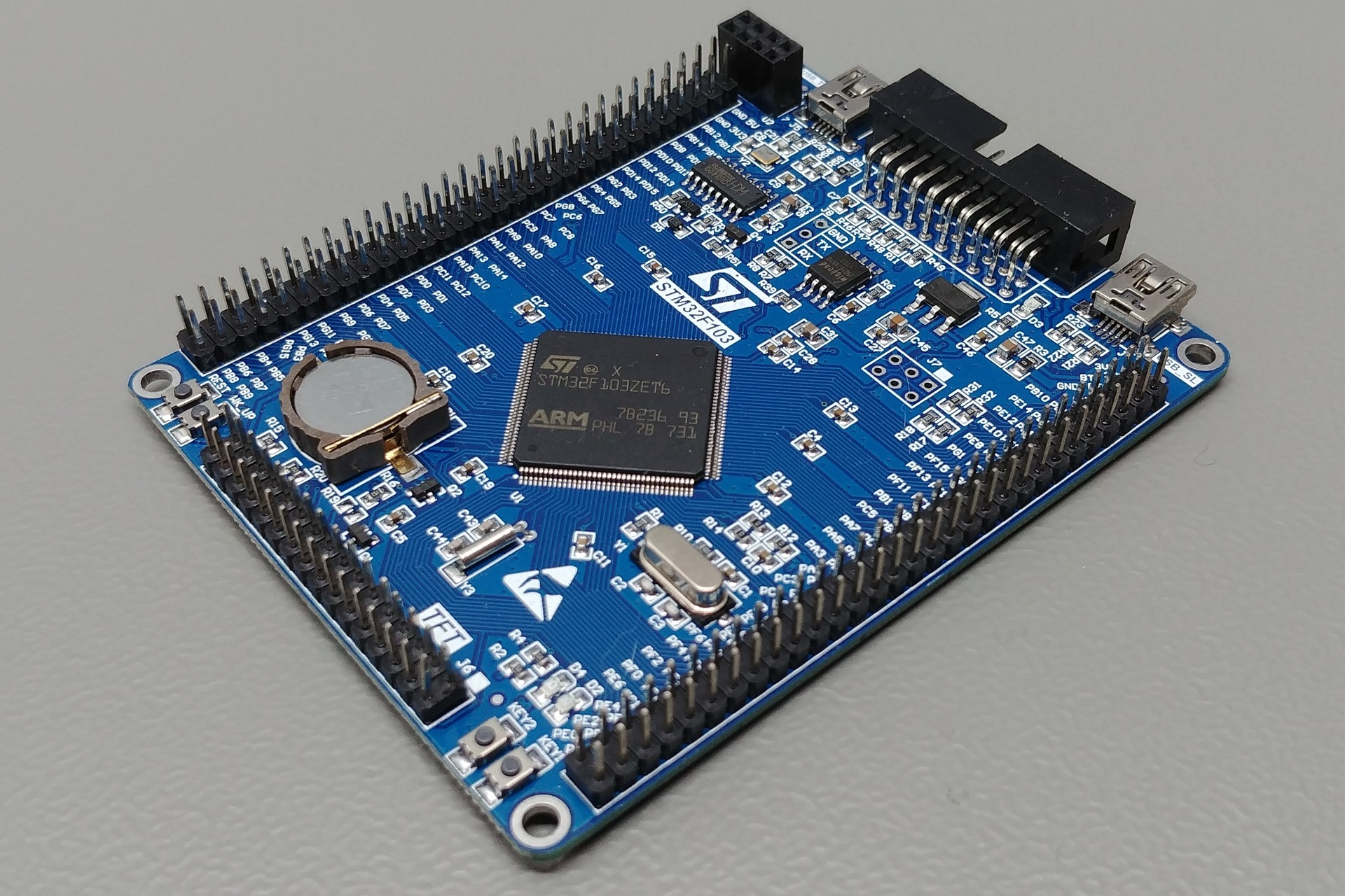
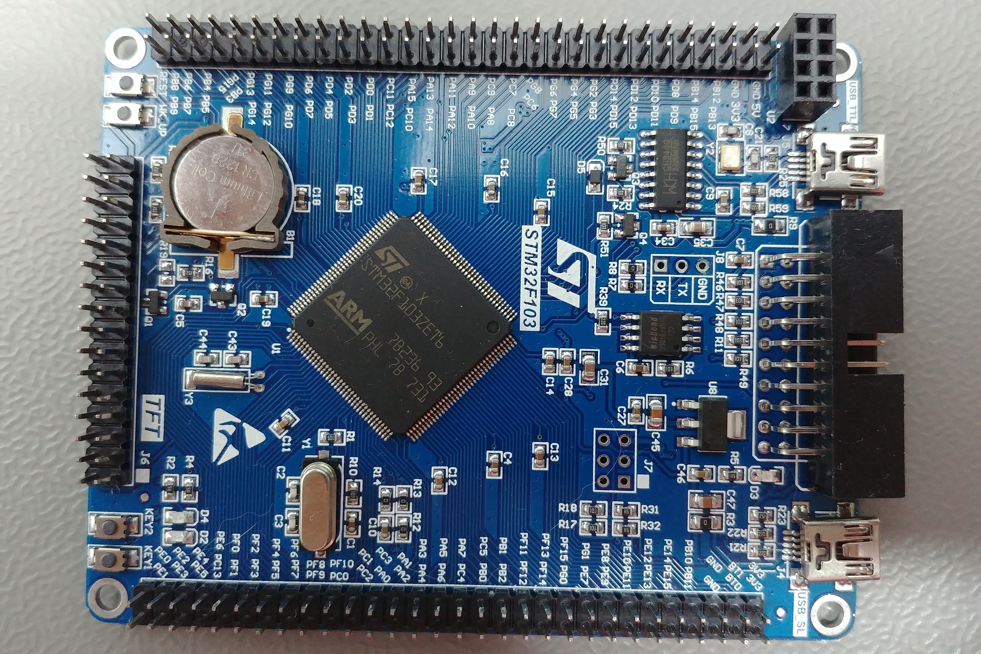
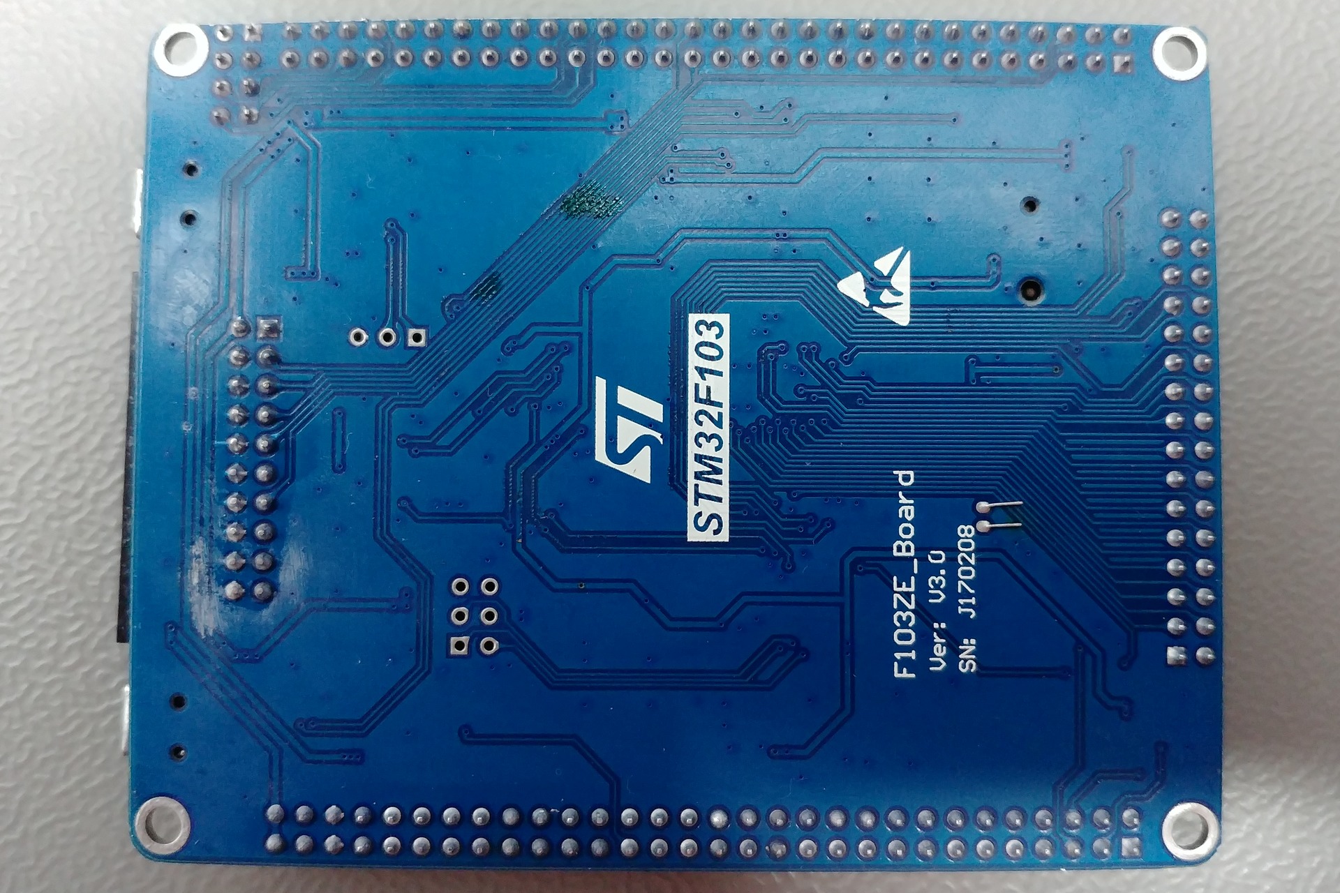
F103ZE board
STM32F103ZET6
Board
| Name | F103ZE board |
| Part | F103ZE_board |
| Brand | Unknown |
| Origin | China |
Microcontroller
| Part | STM32F103ZET6 |
| Manufacturer | ST-Microelectronics |
| Core | Arm Cortex-M3 |
| Max. Clock Speed | 72MHz |
| Package | LQFP 144 pins |
Internal memories
| FLASH | 512KiB |
| SRAM | 64KiB |
Oscillators
| HSI | 8MHz |
| LSI | 40kHz |
| HSE | 8MHz |
| LSE | 32.768kHz |
Power
| Sources | Any +3.3V pin (+3.3V) Any +5V pin (+5V) USB connector (+5V) |
| VDDA pin | No |
| VSSA pin | No |
| VREF- pin | No |
| VREF+ pin | No |
| Backup battery | Holder (12.5mm / 12) |
Regulator
| Manufacturer | Advanced Monolithic Systems Inc. |
| Part | AMS1117 (AMS1117) |
| Package | SOT223 3 pins |
| Input | +4.6V to +15V |
| Output | +3.3V @ 1A |
| Datasheet | AMS1117.pdf |
PCB
| Color | Blue |
| Size (w x l) | 74mm x 95mm |
| Mounting | 4x mounting hole (M3) |
Remarks
- Warning: The +5V pins on this board are directly connected to the +5V pin of the USB connector. There is no protection in place. Do not power this board through USB and an external power supply at the same time.
Pictures
Resources
Outputs
Inputs & outputs
Reset button
| Name | REST |
| Reference | - |
| Type | Button |
| Connected to | NRST |
| Mode | Active low |
BOOT0 jumper
| Name | - |
| Reference | - |
| Type | 2-way jumper |
| Connected to | BOOT0 |
| Mode | N.A. |
- Note: This jumper is part of Header 1.
BOOT1 jumper
| Name | - |
| Reference | - |
| Type | 2-way jumper |
| Connected to | PB2 |
| Mode | N.A. |
- Note: This jumper is part of Header 1.
User button 1
| Name | KEY1 |
| Reference | - |
| Type | Button |
| Connected to | PE2 |
| Mode | Active low |
User button 2
| Name | KEY2 |
| Reference | - |
| Type | Button |
| Connected to | PE1 |
| Mode | Active low |
User button 3
| Name | WK_UP |
| Reference | - |
| Type | Button |
| Connected to | PA0 |
| Mode | Active low |
Power LED
| Name | - |
| Reference | D3 |
| Type | LED |
| Connected to | +3.3V rail |
| Mode | N.A. |
User LED 1
| Name | - |
| Reference | D2 |
| Type | LED |
| Connected to | PE5 |
| Mode | Sink |
User LED 2
| Name | - |
| Reference | D4 |
| Type | LED |
| Connected to | PB5 |
| Mode | Sink |
Connectors & headers
Header 1 properties
| Name | Unknown |
| Reference | None |
| Type | Pin header (2.54mm, 30x2, male) |
Header 1 pins
| # | Name | Function | Connected to |
|---|---|---|---|
| 1 | PE1 | - | PE1 |
| 2 | PE0 | - | PE0 |
| 3 | PE3 | - | PE3 |
| 4 | PE2 | - | PE2 |
| 5 | PE5 | - | PE5 |
| 6 | PE4 | - | PE4 |
| 7 | PC13 | - | PC13 |
| 8 | PE6 | - | PE6 |
| 9 | PF1 | - | PF1 |
| 10 | PF0 | - | PF0 |
| 11 | PF3 | - | PF3 |
| 12 | PF2 | - | PF2 |
| 13 | PF5 | - | PF5 |
| 14 | PF4 | - | PF4 |
| 15 | PF7 | - | PF7 |
| 16 | PF6 | - | PF6 |
| 17 | PF9 | - | PF9 |
| 18 | PF8 | - | PF8 |
| 19 | PC0 | - | PC0 |
| 20 | PF10 | - | PF10 |
| 21 | PC2 | - | PC2 |
| 22 | PC1 | - | PC1 |
| 23 | PA0 | - | PA0 |
| 24 | PC3 | - | PC3 |
| 25 | PA2 | - | PA2 |
| 26 | PA1 | - | PA1 |
| 27 | PA4 | - | PA4 |
| 28 | PA3 | - | PA3 |
| 29 | PA6 | - | PA6 |
| 30 | PA5 | - | PA5 |
| 31 | PC4 | - | PC4 |
| 32 | PA7 | - | PA7 |
| 33 | PB0 | - | PB0 |
| 34 | PC5 | - | PC5 |
| 35 | PB2 | - | PB2 |
| 36 | PB1 | - | PB1 |
| 37 | PF12 | - | PF12 |
| 38 | PF11 | - | PF11 |
| 39 | PF14 | - | PF14 |
| 40 | PF13 | - | PF13 |
| 41 | PG0 | - | PG0 |
| 42 | PF15 | - | PF15 |
| 43 | PE7 | - | PE7 |
| 44 | PG1 | - | PG1 |
| 45 | PE9 | - | PE9 |
| 46 | PE8 | - | PE8 |
| 47 | PE11 | - | PE11 |
| 48 | PE10 | - | PE10 |
| 49 | PE13 | - | PE13 |
| 50 | PE12 | - | PE12 |
| 51 | PE15 | - | PE15 |
| 52 | PE14 | - | PE14 |
| 53 | PB11 | - | PB11 |
| 54 | PB10 | - | PB10 |
| 55 | GND | - | Ground plane |
| 56 | GND | - | Ground plane |
| 57 | BT0 | - | BOOT0 |
| 58 | BT1 | - | PB2 |
| 59 | 3V3 | - | +3.3V rail |
| 60 | 3V3 | - | +3.3V rail |
Header 2 properties
| Name | Unknown |
| Reference | None |
| Type | Pin header (2.54mm, 30x2, male) |
Header 2 pins
| # | Name | Function | Connected to |
|---|---|---|---|
| 1 | PB9 | - | PB9 |
| 2 | PB8 | - | PB8 |
| 3 | PB7 | - | PB7 |
| 4 | PB6 | - | PB6 |
| 5 | PB5 | - | PB5 |
| 6 | PB4 | - | PB4 |
| 7 | PB3 | - | PB3 |
| 8 | PG15 | - | PG15 |
| 9 | PG14 | - | PG14 |
| 10 | PG13 | - | PG13 |
| 11 | PG12 | - | PG12 |
| 12 | PG11 | - | PG11 |
| 13 | PG10 | - | PG10 |
| 14 | PG9 | - | PG9 |
| 15 | PD7 | - | PD7 |
| 16 | PD6 | - | PD6 |
| 17 | PD5 | - | PD5 |
| 18 | PD4 | - | PD4 |
| 19 | PD3 | - | PD3 |
| 20 | PD2 | - | PD2 |
| 21 | PD1 | - | PD1 |
| 22 | PD0 | - | PD0 |
| 23 | PC12 | - | PC12 |
| 24 | PC11 | - | PC11 |
| 25 | PC10 | - | PC10 |
| 26 | PA15 | - | PA15 |
| 27 | PA14 | - | PA14 |
| 28 | PA13 | - | PA13 |
| 29 | PA12 | - | PA12 |
| 30 | PA11 | - | PA11 |
| 31 | PA10 | - | PA10 |
| 32 | PA9 | - | PA9 |
| 33 | PA8 | - | PA8 |
| 34 | PC9 | - | PC9 |
| 35 | PC8 | - | PC8 |
| 36 | PC7 | - | PC7 |
| 37 | PC6 | - | PC6 |
| 38 | PG8 | - | PG8 |
| 39 | PG7 | - | PG7 |
| 40 | PG6 | - | PG6 |
| 41 | PG5 | - | PG5 |
| 42 | PG4 | - | PG4 |
| 43 | PG3 | - | PG3 |
| 44 | PG2 | - | PG2 |
| 45 | PD15 | - | PD15 |
| 46 | PD14 | - | PD14 |
| 47 | PD13 | - | PD13 |
| 48 | PD12 | - | PD12 |
| 49 | PD11 | - | PD11 |
| 50 | PD10 | - | PD10 |
| 51 | PD9 | - | PD9 |
| 52 | PD8 | - | PD8 |
| 53 | PB15 | - | PB15 |
| 54 | PB14 | - | PB14 |
| 55 | PB13 | - | PB13 |
| 56 | PB12 | - | PB12 |
| 57 | 3V3 | - | +3.3V rail |
| 58 | GND | - | Ground plane |
| 59 | 5V | - | +5V rail |
| 60 | GND | - | Ground plane |
Main USB connector properties
| Name | USB_SL |
| Reference | J4 |
| Type | USB Mini |
Main USB connector pins
| # | Name | Function | Connected to |
|---|---|---|---|
| 1 | - | VCC | +5V rail |
| 2 | - | D- | PA11 |
| 3 | - | D+ | PA12 |
| 4 | - | ID | N.C. |
| 5 | - | GND | Ground plane |
Serial USB connector properties
| Name | USB_TTL |
| Reference | J5 |
| Type | USB Mini |
Serial USB connector pins
| # | Name | Function | Connected to |
|---|---|---|---|
| 1 | - | VCC | +5V rail |
| 2 | - | D- | CH340 Pin 6 |
| 3 | - | D+ | CH340 Pin 5 |
| 4 | - | ID | N.C. |
| 5 | - | GND | Ground plane |
JTAG header properties
| Name | Unknown |
| Reference | None |
| Type | IDC (2.54mm, 10x2, male) |
JTAG header pins
| # | Name | Function | Connected to |
|---|---|---|---|
| 1 | - | VCC | +3.3V rail |
| 2 | - | VCC | +3.3V rail |
| 3 | - | TRST | PB4 |
| 4 | - | GND | Ground plane |
| 5 | - | TDI | PA15 |
| 6 | - | GND | Ground plane |
| 7 | - | TMS / SWDIO | PA13 |
| 8 | - | GND | Ground plane |
| 9 | - | TCLK / SWCLK | PA14 |
| 10 | - | GND | Ground plane |
| 11 | - | RTCK | N.C. |
| 12 | - | GND | Ground plane |
| 13 | - | TDO / SWO | PB3 |
| 14 | - | GND | Ground plane |
| 15 | - | RESET | NRST |
| 16 | - | GND | Ground plane |
| 17 | - | N.C. | N.C. |
| 18 | - | GND | Ground plane |
| 19 | - | N.C. | N.C. |
| 20 | - | GND | Ground plane |
TFT LCD header properties
| Name | TFT |
| Reference | J3 |
| Type | Pin header (2.54mm, 16x2, female) |
- Note: Pin 28 is used for controlling the TFT backlight. It is connected to the collector of Q1. The emitter of Q1 is connected to the +3.3V rail. The base of Q1 is connected to the absent resistor R19. Neither side of R19 is connected to the microcontroller. By default, the base of Q1 is in a floating state, and does not conduct. Pin 28 is pulled down by a 1.5kΩ resistor (R20). To make the signal on pin 28 high, you can either install a 100Ω 0603 resistor as R19 or connect the base to one of the microcontroller's pins through a 1.5kΩ resistor.
- Note: Pin 29 is usually not connected on the TFT side.
TFT LCD header pins
| # | Name | Function | Connected to |
|---|---|---|---|
| 1 | - | GND | Ground plane |
| 2 | - | RST | Reset button |
| 3 | - | FSMC D15 | PD10 |
| 4 | - | FSMC D14 | PD9 |
| 5 | - | FSMC D13 | PD8 |
| 6 | - | FSMC D12 | PE15 |
| 7 | - | FSMC D11 | PE14 |
| 8 | - | FSMC D10 | PE13 |
| 9 | - | FSMC D9 | PE12 |
| 10 | - | FSMC D8 | PE11 |
| 11 | - | FSMC D7 | PE10 |
| 12 | - | FSMC D6 | PE9 |
| 13 | - | FSMC D5 | PE8 |
| 14 | - | FSMC D4 | PE7 |
| 15 | - | FSMC D3 | PD1 |
| 16 | - | FSMC D2 | PD0 |
| 17 | - | FSMC D1 | PD15 |
| 18 | - | FSMC D0 | PD14 |
| 19 | - | FSMC NOE | PD4 |
| 20 | - | FSMC NWE | PD5 |
| 21 | - | FSMC A10 | PG0 |
| 22 | - | FSMC NE4 | PG12 |
| 23 | - | Touch CLK | PB1 |
| 24 | - | Touch CS | PB2 |
| 25 | - | Touch MOSI | PF9 |
| 26 | - | Touch MISO | PF8 |
| 27 | - | Touch PEN | PC13 via R15 (1.5kΩ) |
| 28 | - | LCD Backlight | Q1 collector |
| 29 | - | VBAT | VBAT |
| 30 | - | GND | Ground plane |
| 31 | - | 3V3 | +3.3V rail |
| 32 | - | GND | Ground plane |
nRF24L01 module header properties
| Name | Unknown |
| Reference | None |
| Type | Pin header (2.54mm, 4x2, female) |
nRF24L01 module header pins
| # | Name | Function | Connected to |
|---|---|---|---|
| 1 | - | GND | Ground plane |
| 2 | - | VCC | +3.3V rail |
| 3 | - | CE | PG6 |
| 4 | - | CSN | PG7 |
| 5 | - | SCK | PB13 |
| 6 | - | MOSI | PB15 |
| 7 | - | MISO | PB14 |
| 8 | - | IRQ | PG8 |
Devices
CH340 pins
| # | Name | Function | Connected to |
|---|---|---|---|
| 1 | - | GND | Ground plane |
| 2 | - | TXD | PA9 |
| 3 | - | RXD | PA10 |
| 4 | - | V3 | N.C. |
| 5 | - | UD+ | D+ pin on Main USB connector |
| 6 | - | UD- | D- pin on Main USB connector |
| 7 | - | XI | Crystal Y1 |
| 8 | - | XO | Crystal Y1 |
| 9 | - | CTS# | N.C. |
| 10 | - | DSR# | N.C. |
| 11 | - | RI# | N.C. |
| 12 | - | DCD# | N.C. |
| 13 | - | DTR# | Unknown |
| 14 | - | RTS# | Unknown |
| 15 | - | R232 | N.C. |
| 16 | - | VCC | N.C. |
W25Q16JV properties
| Name | FLASH |
| Reference | U3 |
| Manufacturer | Winbond Electronics Corporation |
| Part | W25Q16JV |
| Marking | W25Q16JVSIQ |
| Datasheet | W25Q16JV.pdf |
| Package | SOIC 8 pins |
| Description | 2MiB Dual/Quad SPI FLASH |
W25Q16JV pins
| # | Name | Function | Connected to |
|---|---|---|---|
| 1 | - | /CS | PB12 |
| 2 | - | DO | PB14 |
| 3 | - | /WP | +3.3V rail |
| 4 | - | GND | Ground plane |
| 5 | - | DI | PB15 |
| 6 | - | CLK | PB13 |
| 7 | - | /HOLD | +3.3V rail |
| 8 | - | VCC | +3.3V rail |