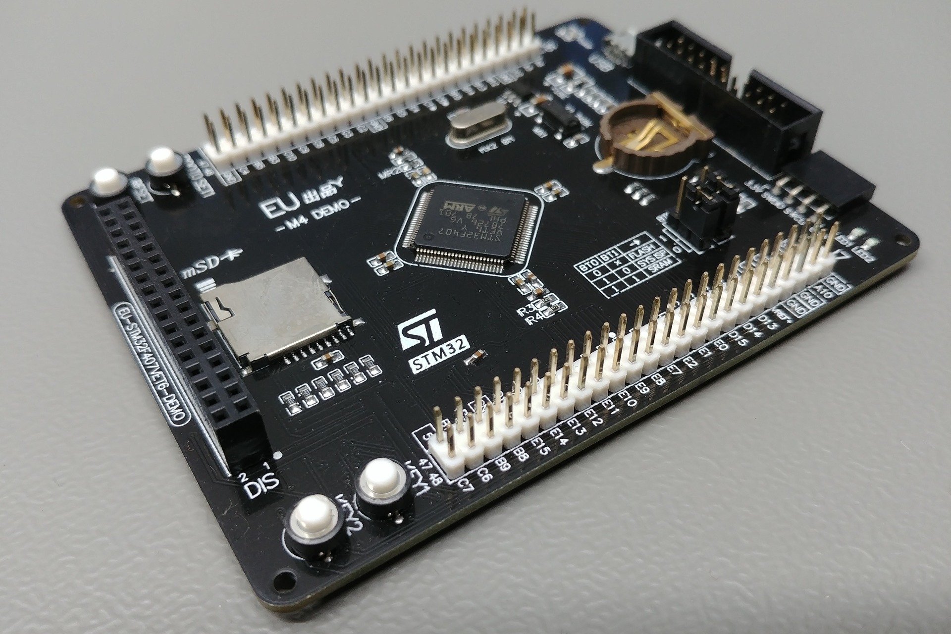
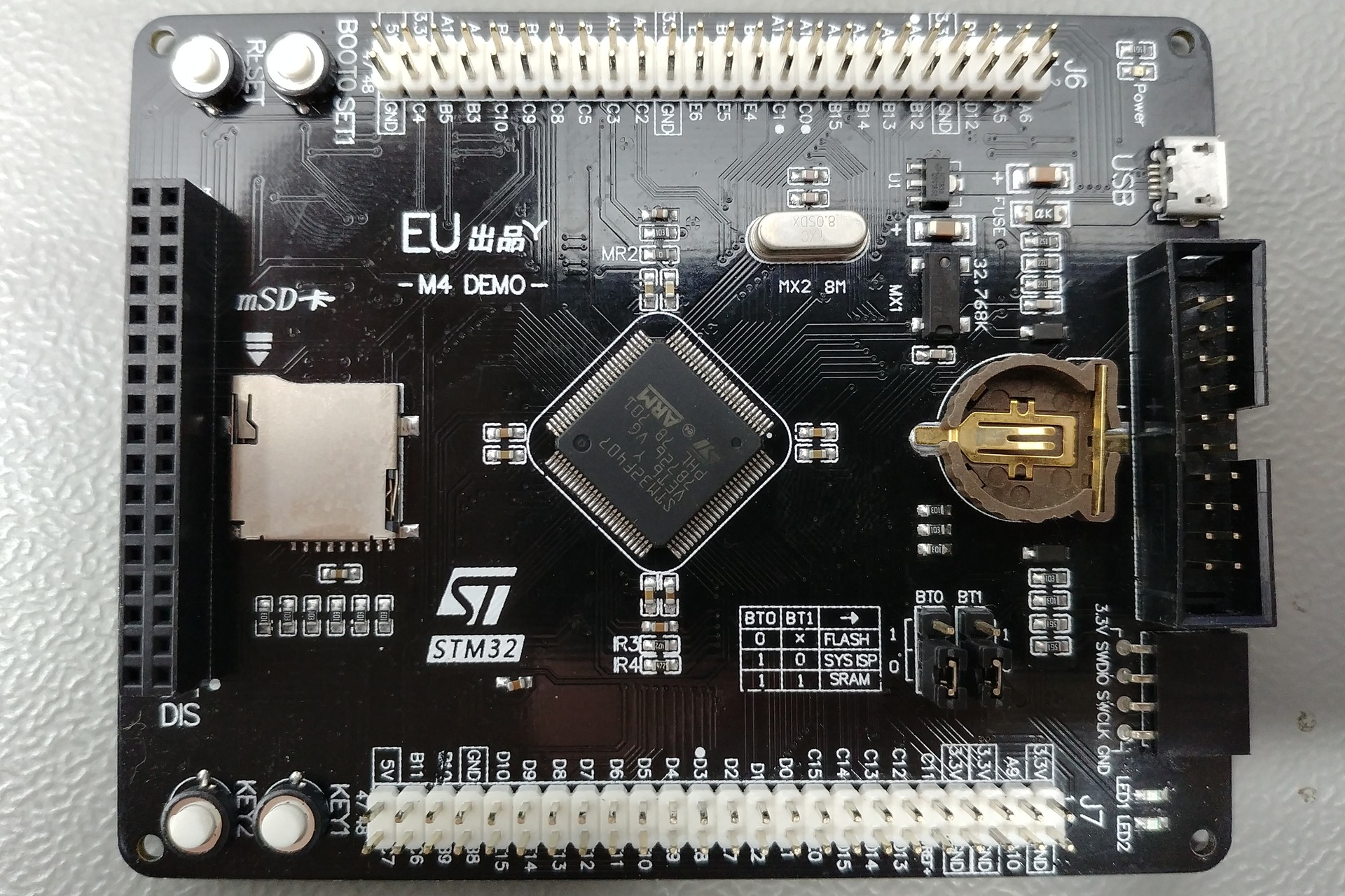
Euse M4 DEMO
STM32F407VET6
Board
| Name | Euse M4 DEMO |
| Part | EU-STM32F407VET6-DEMO |
| Brand | Euse |
| Origin | China |
Microcontroller
| Part | STM32F407VET6 |
| Manufacturer | ST-Microelectronics |
| Core | Arm Cortex-M4 |
| Max. Clock Speed | 168MHz |
| Package | LQFP 100 pins |
Internal memories
| FLASH | 512KiB |
| SRAM | 192KiB |
| Backup SRAM | 4KiB |
Oscillators
| HSI | 16MHz |
| LSI | 32kHz |
| HSE | 8MHz |
| LSE | 32.768kHz |
Power
| Sources | Any +3.3V pin (+3.3V) Any +5V pin (+5V) USB connector (+5V) |
| VDDA pin | No |
| VSSA pin | No |
| VREF- pin | No |
| VREF+ pin | Yes |
| Backup battery | Holder (12.5mm / 12) |
Regulator
| Manufacturer | Holtek Semiconductor Inc. |
| Part | HT7833 (HT7833) |
| Package | SOT89-3 3 pins |
| Input | +4.3V to +8.5V |
| Output | +3.3V @ 500mA |
| Datasheet | HT78xx.pdf |
PCB
| Color | Black |
| Size (w x l) | 69mm x 101mm |
| Mounting | 4x mounting hole (M2) |
Remarks
- Warning: The +5V pins on this board are directly connected to the +5V pin of the USB connector. There is no protection in place. Do not power this board through USB and an external power supply at the same time.
- Warning: The microcontroller on this board features internal pull-up resistors for the USB data lines. However, this board has an additional pull-up resistor on D+. This resistor is not needed and violates the USB specification when the internal pull-up resistors are also used. This may cause errors while using USB on this board.
Pictures
Resources
Outputs
Devices
Inputs & outputs
Reset button
| Name | RESET |
| Reference | - |
| Type | Button |
| Connected to | NRST |
| Mode | Active low |
BOOT0 jumper
| Name | BT0 |
| Reference | - |
| Type | 2-way jumper |
| Connected to | BOOT0 |
| Mode | N.A. |
BOOT1 jumper
| Name | BT1 |
| Reference | - |
| Type | 2-way jumper |
| Connected to | PB2 |
| Mode | N.A. |
BOOT0 button
| Name | BOOT0 SET1 |
| Reference | - |
| Type | Button |
| Connected to | BOOT0 |
| Mode | Active high |
User button 1
| Name | KEY1 |
| Reference | - |
| Type | Button |
| Connected to | PA0 |
| Mode | Active high |
User button 2
| Name | KEY2 |
| Reference | - |
| Type | Button |
| Connected to | PC1 |
| Mode | Active high |
DIS NC solder bridges
| Name | - |
| Reference | - |
| Type | Solder bridge |
| Connected to | Display header NC pin |
| Mode | N.A. |
- Info: Connects the Display NC pin to either +5V, +3.3V or ground.
Power LED
| Name | Power |
| Reference | - |
| Type | LED |
| Connected to | +3.3V rail |
| Mode | N.A. |
User LED 1
| Name | LED1 |
| Reference | - |
| Type | LED |
| Connected to | PC0 |
| Mode | Sink |
User LED 2
| Name | LED2 |
| Reference | - |
| Type | LED |
| Connected to | PD3 |
| Mode | Sink |
Connectors & headers
Header 1 properties
| Name | Unknown |
| Reference | J7 |
| Type | Pin header (2.54mm, 24x2, male) |
Header 1 pins
| # | Name | Function | Connected to |
|---|---|---|---|
| 1 | 3.3V | - | +3.3V rail |
| 2 | GND | - | Ground plane |
| 3 | A9 | - | PA9 |
| 4 | A10 | - | PA10 |
| 5 | 3.3V | - | +3.3V rail |
| 6 | GND | - | Ground plane |
| 7 | 3.3V | - | +3.3V rail |
| 8 | GND | - | Ground plane |
| 9 | C11 | - | PC11 |
| 10 | VREF+ | - | VREF+ |
| 11 | C12 | - | PC12 |
| 12 | D13 | - | PD13 |
| 13 | C13 | - | PC13 |
| 14 | D14 | - | PD14 |
| 15 | C14 | - | PC14 |
| 16 | D15 | - | PD15 |
| 17 | C15 | - | PC15 |
| 18 | E0 | - | PE0 |
| 19 | D0 | - | PD0 |
| 20 | E1 | - | PE1 |
| 21 | D1 | - | PD1 |
| 22 | E2 | - | PE2 |
| 23 | D2 | - | PD2 |
| 24 | E7 | - | PE7 |
| 25 | D3 | - | PD3 |
| 26 | E8 | - | PE8 |
| 27 | D4 | - | PD4 |
| 28 | E9 | - | PE9 |
| 29 | D5 | - | PD5 |
| 30 | E10 | - | PE10 |
| 31 | D6 | - | PD6 |
| 32 | E11 | - | PE11 |
| 33 | D7 | - | PD7 |
| 34 | E12 | - | PE12 |
| 35 | D8 | - | PD8 |
| 36 | E13 | - | PE13 |
| 37 | D9 | - | PD9 |
| 38 | E14 | - | PE14 |
| 39 | D10 | - | PD10 |
| 40 | E15 | - | PE15 |
| 41 | GND | - | Ground plane |
| 42 | B8 | - | PB8 |
| 43 | B10 | - | PB10 |
| 44 | B9 | - | PB9 |
| 45 | B11 | - | PB11 |
| 46 | C6 | - | PC6 |
| 47 | 5V | - | +5V rail |
| 48 | C7 | - | PC7 |
Header 2 properties
| Name | Unknown |
| Reference | J6 |
| Type | Pin header (2.54mm, 24x2, male) |
Header 2 pins
| # | Name | Function | Connected to |
|---|---|---|---|
| 1 | A8 | - | PA8 |
| 2 | A6 | - | PA6 |
| 3 | A7 | - | PA7 |
| 4 | A5 | - | PA5 |
| 5 | D11 | - | PD11 |
| 6 | D12 | - | PD12 |
| 7 | 3.3V | - | +3.3V rail |
| 8 | GND | - | Ground plane |
| 9 | A0 | - | PA0 |
| 10 | B12 | - | PB12 |
| 11 | A1 | - | PA1 |
| 12 | B13 | - | PB13 |
| 13 | A2 | - | PA2 |
| 14 | B14 | - | PB14 |
| 15 | A3 | - | PA3 |
| 16 | B15 | - | PB15 |
| 17 | A11 | - | PA11 |
| 18 | C0 | - | PC0 |
| 19 | A12 | - | PA12 |
| 20 | C1 | - | PC1 |
| 21 | B6 | - | PB6 |
| 22 | E4 | - | PE4 |
| 23 | B7 | - | PB7 |
| 24 | E5 | - | PE5 |
| 25 | E3 | - | PE3 |
| 26 | E6 | - | PE6 |
| 27 | 3.3V | - | +3.3V rail |
| 28 | GND | - | Ground plane |
| 29 | A13 | - | PA13 |
| 30 | C2 | - | PC2 |
| 31 | A14 | - | PA14 |
| 32 | C3 | - | PC3 |
| 33 | B0 | - | PB0 |
| 34 | C5 | - | PC5 |
| 35 | B1 | - | PB1 |
| 36 | C8 | - | PC8 |
| 37 | B2 | - | PB2 |
| 38 | C9 | - | PC9 |
| 39 | B4 | - | PB4 |
| 40 | C10 | - | PC10 |
| 41 | A4 | - | PA4 |
| 42 | B3 | - | PB3 |
| 43 | A15 | - | PA15 |
| 44 | B5 | - | PB5 |
| 45 | 3.3V | - | +3.3V rail |
| 46 | C4 | - | PC4 |
| 47 | 5V | - | +5V rail |
| 48 | GND | - | Ground plane |
USB connector properties
| Name | USB |
| Reference | None |
| Type | USB Micro |
USB connector pins
| # | Name | Function | Connected to |
|---|---|---|---|
| 1 | - | VCC | +5V rail |
| 2 | - | D- | PA11 |
| 3 | - | D+ | PA12 |
| 4 | - | ID | N.C. |
| 5 | - | GND | Ground plane |
SWD header properties
| Name | Unknown |
| Reference | None |
| Type | Pin header (2.54mm, 4x1, female) |
SWD header pins
| # | Name | Function | Connected to |
|---|---|---|---|
| 1 | 3.3V | VCC | +3.3V rail |
| 2 | SWDIO | SWDIO | PA13 |
| 3 | SWCLK | SWCLK | PA14 |
| 4 | GND | GND | Ground plane |
JTAG header properties
| Name | Unknown |
| Reference | None |
| Type | IDC (2.54mm, 10x2, male) |
JTAG header pins
| # | Name | Function | Connected to |
|---|---|---|---|
| 1 | - | VCC | +3.3V rail |
| 2 | - | VCC | +3.3V rail |
| 3 | - | TRST | PB4 |
| 4 | - | GND | Ground plane |
| 5 | - | TDI | PA15 |
| 6 | - | GND | Ground plane |
| 7 | - | TMS / SWDIO | PA13 |
| 8 | - | GND | Ground plane |
| 9 | - | TCLK / SWCLK | PA14 |
| 10 | - | GND | Ground plane |
| 11 | - | RTCK | N.C. |
| 12 | - | GND | Ground plane |
| 13 | - | TDO / SWO | PB3 |
| 14 | - | GND | Ground plane |
| 15 | - | RESET | NRST |
| 16 | - | GND | Ground plane |
| 17 | - | N.C. | N.C. |
| 18 | - | GND | Ground plane |
| 19 | - | N.C. | N.C. |
| 20 | - | GND | Ground plane |
SD-card connector properties
| Name | mSD |
| Reference | None |
| Type | microSD |
SD-card connector pins
| # | Name | Function | Connected to |
|---|---|---|---|
| 1 | - | DAT2 | N.C. |
| 2 | - | CD/DAT3 | PC11 |
| 3 | - | CMD | PD2 |
| 4 | - | VDD | +3.3V rail |
| 5 | - | CLK | PC12 |
| 6 | - | VSS | Ground plane |
| 7 | - | DAT0 | PC8 |
| 8 | - | DAT1 | N.C. |
| 9 | - | CD | N.C. |
| 10 | - | Body | Ground plane |
TFT header properties
| Name | DIS |
| Reference | None |
| Type | Pin header (2.54mm, 17x2, female) |
TFT header pins
| # | Name | Function | Connected to |
|---|---|---|---|
| 1 | D7 | - | PD7 |
| 2 | D13 | - | PD13 |
| 3 | D5 | - | PD5 |
| 4 | D4 | - | PD4 |
| 5 | C5 | - | PC5 |
| 6 | D14 | - | PD14 |
| 7 | D15 | - | PD15 |
| 8 | D0 | - | PD0 |
| 9 | D1 | - | PD1 |
| 10 | E7 | - | PE7 |
| 11 | E8 | - | PE8 |
| 12 | E9 | - | PE9 |
| 13 | E10 | - | PE10 |
| 14 | E11 | - | PE11 |
| 15 | E12 | - | PE12 |
| 16 | E13 | - | PE13 |
| 17 | E14 | - | PE14 |
| 18 | E15 | - | PE15 |
| 19 | D8 | - | PD8 |
| 20 | D9 | - | PD9 |
| 21 | D10 | - | PD10 |
| 22 | C2 | - | PC2 |
| 23 | B0 | - | PB0 |
| 24 | 3.3V | - | +3.3V rail |
| 25 | 3.3V | - | +3.3V rail |
| 26 | GND | - | Ground plane |
| 27 | GND | - | Ground plane |
| 28 | NC | - | N.C. |
| 29 | E0 | - | PE0 |
| 30 | E1 | - | PE1 |
| 31 | E2 | - | PE2 |
| 32 | C3 | - | PC3 |
| 33 | B2 | - | PB2 |
| 34 | B1 | - | PB1 |
Devices
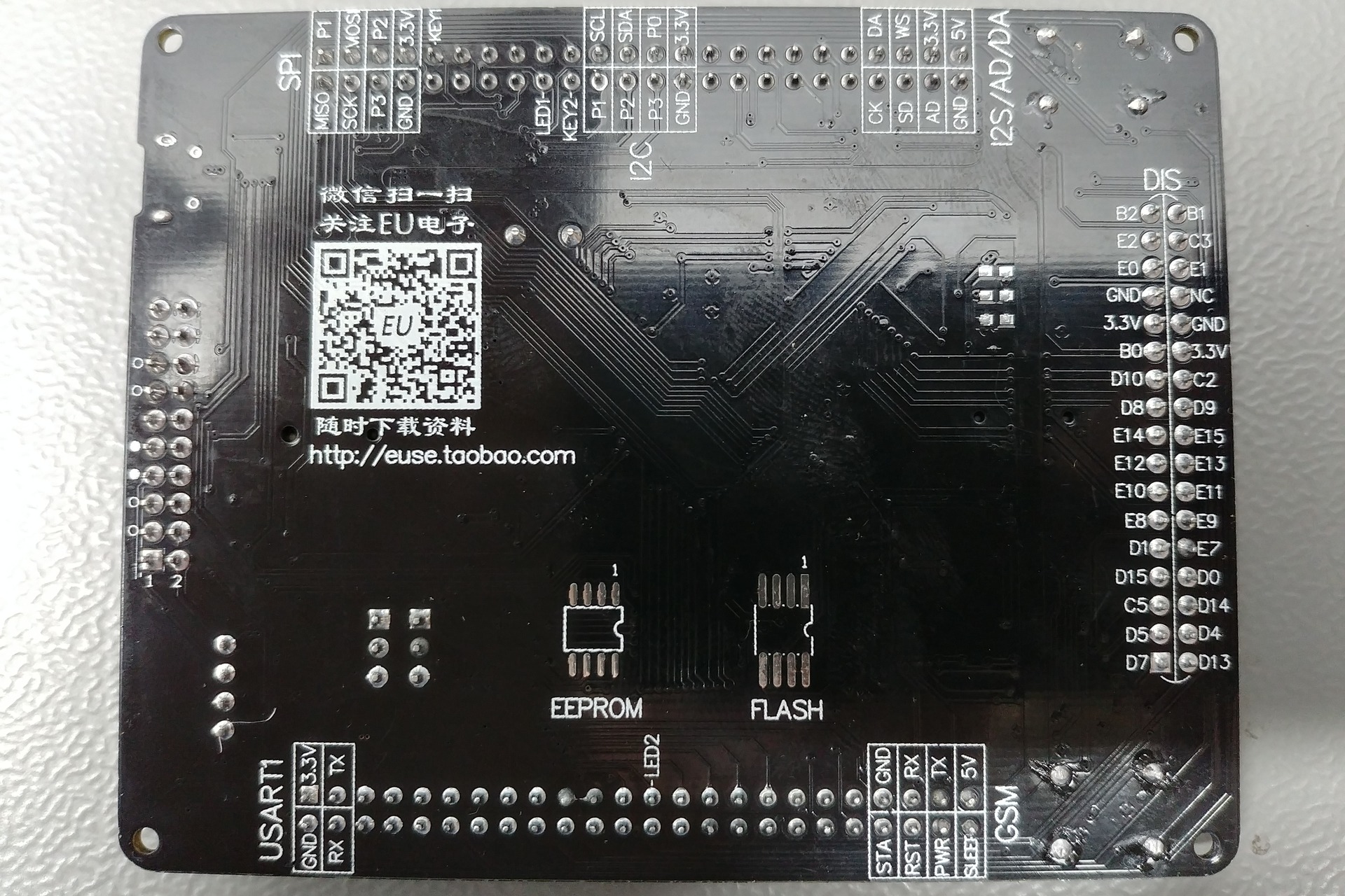
Generic EEPROM properties footprint
| Name | EEPROM |
| Reference | Unknown |
| Manufacturer | Unknown |
| Part | Generic EEPROM |
| Marking | Unknown |
| Datasheet | Unavailable |
| Package | SOP 8 pins |
| Description | Generic I2C EEPROM |
Generic EEPROM pins footprint
| # | Name | Function | Connected to |
|---|---|---|---|
| 1 | - | A0 | Ground plane |
| 2 | - | A1 | Ground plane |
| 3 | - | A2 | Ground plane |
| 4 | - | GND | Ground plane |
| 5 | - | SDA | PB7 |
| 6 | - | SCL | PB6 |
| 7 | - | WP | Ground plane |
| 8 | - | VCC | +3.3V rail |
Generic FLASH properties footprint
| Name | FLASH |
| Reference | Unknown |
| Manufacturer | Unknown |
| Part | Generic FLASH |
| Marking | Unknown |
| Datasheet | Unavailable |
| Package | SOIC 8 pins |
| Description | Generic Dual/Quad SPI FLASH |
Generic FLASH pins footprint
| # | Name | Function | Connected to |
|---|---|---|---|
| 1 | - | CS | PB12 |
| 2 | - | DO | PB14 |
| 3 | - | WP | +3.3V rail |
| 4 | - | GND | Ground plane |
| 5 | - | DI | PB15 |
| 6 | - | CLK | PB13 |
| 7 | - | HOLD | +3.3V rail |
| 8 | - | VCC | +3.3V rail |