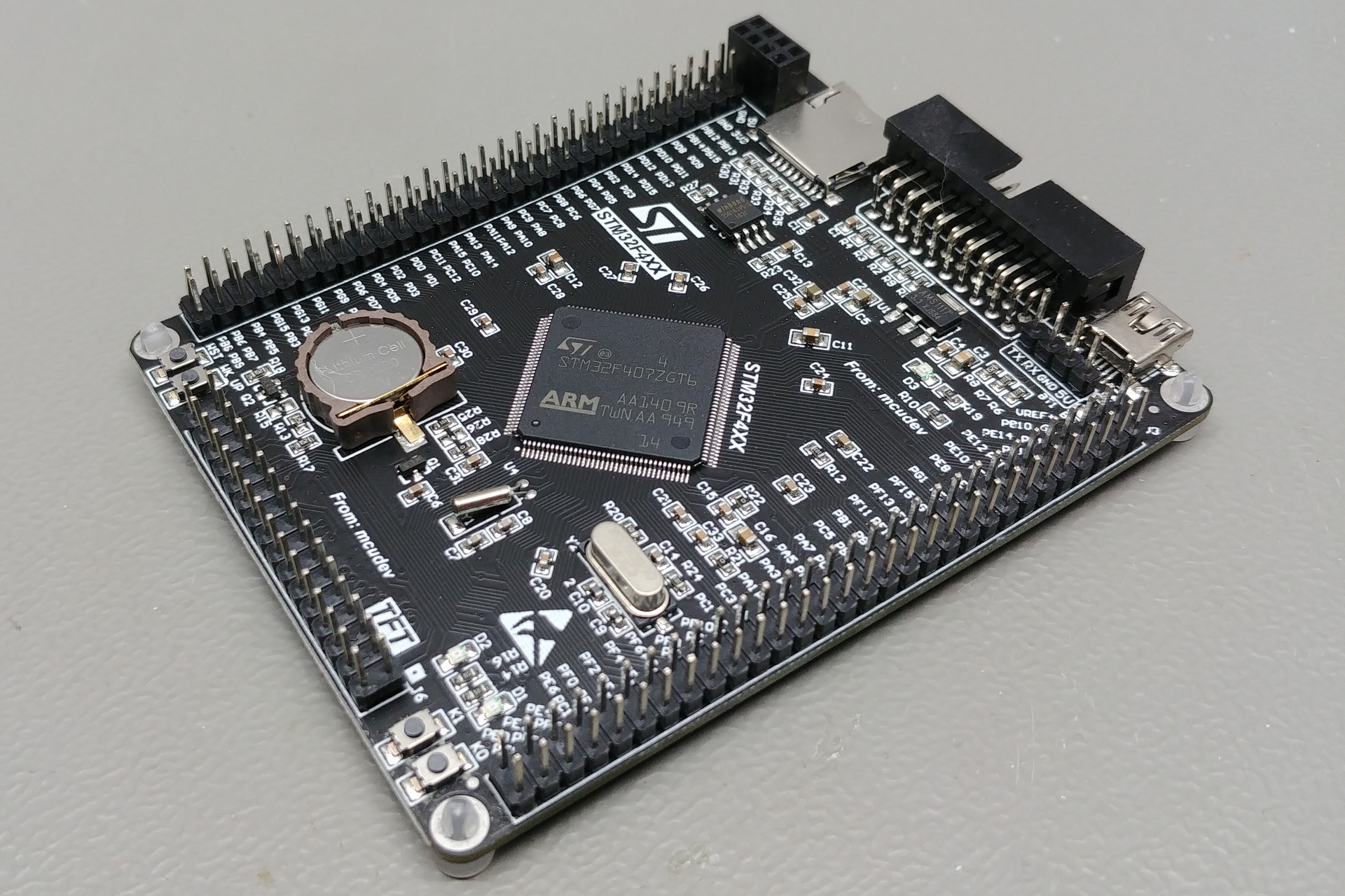
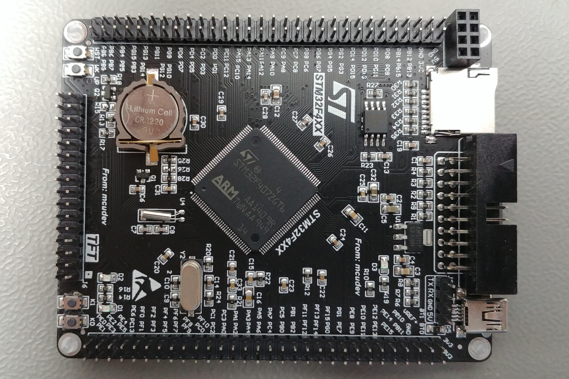
STM32F4XX
Board
| Name | STM32F4XX |
| Part | STM32_F4XX |
| Brand | Unknown |
| Origin | China |
Internal memories
| FLASH | KiB |
| SRAM | KiB |
Oscillators
| HSI | MHz |
| LSI | kHz |
| HSE | 8MHz |
| LSE | 32.768kHz |
Power
| Sources | Any +3.3V pin (+3.3V) Any +5V pin (+5V) USB connector (+5V) |
| VDDA pin | No |
| VSSA pin | No |
| VREF- pin | No |
| VREF+ pin | No |
| Backup battery | Holder (12.5mm / 12) |
Regulator
| Manufacturer | Advanced Monolithic Systems Inc. |
| Part | AMS1117 (AMS1117) |
| Package | SOT223 3 pins |
| Input | +4.6V to +15V |
| Output | +3.3V @ 1A |
| Datasheet | AMS1117.pdf |
PCB
| Color | Black |
| Size (w x l) | 64mm x 95mm |
| Mounting | 4x mounting hole (M3) |
Remarks
- Warning: The +5V pins on this board are directly connected to the +5V pin of the USB connector. There is no protection in place. Do not power this board through USB and an external power supply at the same time.
- Note: When installing U2, make sure to also install R29 (10kΩ), C17 (0.1μF), and C18 (0.1μF).
Pictures
Outputs
Devices
Inputs & outputs
Reset button
| Name | RST |
| Reference | - |
| Type | Button |
| Connected to | NRST |
| Mode | Active low |
User button 1
| Name | K0 |
| Reference | - |
| Type | Button |
| Connected to | PE4 |
| Mode | Active low |
User button 2
| Name | K1 |
| Reference | - |
| Type | Button |
| Connected to | PE3 |
| Mode | Active low |
User button 3
| Name | WK_UP |
| Reference | - |
| Type | Button |
| Connected to | PA0 |
| Mode | Active high |
Power LED
| Name | - |
| Reference | D3 |
| Type | LED |
| Connected to | +3.3V rail |
| Mode | N.A. |
User LED 1
| Name | - |
| Reference | D1 |
| Type | LED |
| Connected to | PF9 |
| Mode | Sink |
User LED 2
| Name | - |
| Reference | D2 |
| Type | LED |
| Connected to | PF10 |
| Mode | Sink |
Connectors & headers
Header 1 properties
| Name | Unknown |
| Reference | None |
| Type | Pin header (2.54mm, 30x2, male) |
Header 1 pins
| # | Name | Function | Connected to |
|---|---|---|---|
| 1 | PE1 | - | PE1 |
| 2 | PE0 | - | PE0 |
| 3 | PE3 | - | PE3 |
| 4 | PE2 | - | PE2 |
| 5 | PE5 | - | PE5 |
| 6 | PE4 | - | PE4 |
| 7 | PC13 | - | PC13 |
| 8 | PE6 | - | PE6 |
| 9 | PF1 | - | PF1 |
| 10 | PF0 | - | PF0 |
| 11 | PF3 | - | PF3 |
| 12 | PF2 | - | PF2 |
| 13 | PF5 | - | PF5 |
| 14 | PF4 | - | PF4 |
| 15 | PF7 | - | PF7 |
| 16 | PF6 | - | PF6 |
| 17 | PF9 | - | PF9 |
| 18 | PF8 | - | PF8 |
| 19 | PC0 | - | PC0 |
| 20 | PF10 | - | PF10 |
| 21 | PC2 | - | PC2 |
| 22 | PC1 | - | PC1 |
| 23 | PA0 | - | PA0 |
| 24 | PC3 | - | PC3 |
| 25 | PA2 | - | PA2 |
| 26 | PA1 | - | PA1 |
| 27 | PA4 | - | PA4 |
| 28 | PA3 | - | PA3 |
| 29 | PA6 | - | PA6 |
| 30 | PA5 | - | PA5 |
| 31 | PC4 | - | PC4 |
| 32 | PA7 | - | PA7 |
| 33 | PB0 | - | PB0 |
| 34 | PC5 | - | PC5 |
| 35 | PB2 | - | PB2 |
| 36 | PB1 | - | PB1 |
| 37 | PF12 | - | PF12 |
| 38 | PF11 | - | PF11 |
| 39 | PF14 | - | PF14 |
| 40 | PF13 | - | PF13 |
| 41 | PG0 | - | PG0 |
| 42 | PF15 | - | PF15 |
| 43 | PE7 | - | PE7 |
| 44 | PG1 | - | PG1 |
| 45 | PE9 | - | PE9 |
| 46 | PE6 | - | PE6 |
| 47 | PE11 | - | PE11 |
| 48 | PE10 | - | PE10 |
| 49 | PE13 | - | PE13 |
| 50 | PE12 | - | PE12 |
| 51 | PE15 | - | PE15 |
| 52 | PE14 | - | PE14 |
| 53 | PB11 | - | PB11 |
| 54 | PB10 | - | PB10 |
| 55 | GND | - | Ground plane |
| 56 | VREF+ | - | VREF+ |
| 57 | BT0 | - | BOOT0 |
| 58 | BT1 | - | PB2 |
| 59 | 3V3 | - | +3.3V rail |
| 60 | 3V3 | - | +3.3V rail |
Header 2 properties
| Name | Unknown |
| Reference | None |
| Type | Pin header (2.54mm, 30x2, male) |
Header 2 pins
| # | Name | Function | Connected to |
|---|---|---|---|
| 1 | PB9 | - | PB9 |
| 2 | PB8 | - | PB8 |
| 3 | PB7 | - | PB7 |
| 4 | PB6 | - | PB6 |
| 5 | PB5 | - | PB5 |
| 6 | PB4 | - | PB4 |
| 7 | PB3 | - | PB3 |
| 8 | PG15 | - | PG15 |
| 9 | PG14 | - | PG14 |
| 10 | PG13 | - | PG13 |
| 11 | PG12 | - | PG12 |
| 12 | PG11 | - | PG11 |
| 13 | PG10 | - | PG10 |
| 14 | PB9 | - | PB9 |
| 15 | PD7 | - | PD7 |
| 16 | PD6 | - | PD6 |
| 17 | PD5 | - | PD5 |
| 18 | PD4 | - | PD4 |
| 19 | PD3 | - | PD3 |
| 20 | PD2 | - | PD2 |
| 21 | PD1 | - | PD1 |
| 22 | PD0 | - | PD0 |
| 23 | PC12 | - | PC12 |
| 24 | PC11 | - | PC11 |
| 25 | PC10 | - | PC10 |
| 26 | PA15 | - | PA15 |
| 27 | PA14 | - | PA14 |
| 28 | PA13 | - | PA13 |
| 29 | PA12 | - | PA12 |
| 30 | PA11 | - | PA11 |
| 31 | PA10 | - | PA10 |
| 32 | PA9 | - | PA9 |
| 33 | PA8 | - | PA8 |
| 34 | PC9 | - | PC9 |
| 35 | PC8 | - | PC8 |
| 36 | PC7 | - | PC7 |
| 37 | PC6 | - | PC6 |
| 38 | PG8 | - | PG8 |
| 39 | PG7 | - | PG7 |
| 40 | PG6 | - | PG6 |
| 41 | PG5 | - | PG5 |
| 42 | PG4 | - | PG4 |
| 43 | PG3 | - | PG3 |
| 44 | PG2 | - | PG2 |
| 45 | PD15 | - | PD15 |
| 46 | PD14 | - | PD14 |
| 47 | PD13 | - | PD13 |
| 48 | PD12 | - | PD12 |
| 49 | PD11 | - | PD11 |
| 50 | PD10 | - | PD10 |
| 51 | PD9 | - | PD9 |
| 52 | PD8 | - | PD8 |
| 53 | PB15 | - | PB15 |
| 54 | PB14 | - | PB14 |
| 55 | PB13 | - | PB13 |
| 56 | PB12 | - | PB12 |
| 57 | 3V3 | - | +3.3V rail |
| 58 | GND | - | Ground plane |
| 59 | 5V | - | +5V rail |
| 60 | GND | - | Ground plane |
USB connector properties
| Name | Unknown |
| Reference | None |
| Type | USB Mini |
USB connector pins
| # | Name | Function | Connected to |
|---|---|---|---|
| 1 | - | VCC | +5V rail |
| 2 | - | D- | PA11 |
| 3 | - | D+ | PA12 |
| 4 | - | ID | N.C. |
| 5 | - | GND | Ground plane |
JTAG header properties
| Name | Unknown |
| Reference | None |
| Type | IDC (2.54mm, 10x2, male) |
JTAG header pins
| # | Name | Function | Connected to |
|---|---|---|---|
| 1 | - | VCC | +3.3V rail |
| 2 | - | VCC | +3.3V rail |
| 3 | - | TRST | PB4 |
| 4 | - | GND | Ground plane |
| 5 | - | TDI | PA15 |
| 6 | - | GND | Ground plane |
| 7 | - | TMS / SWDIO | PA13 |
| 8 | - | GND | Ground plane |
| 9 | - | TCLK / SWCLK | PA14 |
| 10 | - | GND | Ground plane |
| 11 | - | RTCK | N.C. |
| 12 | - | GND | Ground plane |
| 13 | - | TDO / SWO | PB3 |
| 14 | - | GND | Ground plane |
| 15 | - | RESET | NRST |
| 16 | - | GND | Ground plane |
| 17 | - | N.C. | N.C. |
| 18 | - | GND | Ground plane |
| 19 | - | N.C. | N.C. |
| 20 | - | GND | Ground plane |
SD-card connector properties
| Name | Unknown |
| Reference | None |
| Type | microSD |
SD-card connector pins
| # | Name | Function | Connected to |
|---|---|---|---|
| 1 | - | DAT2 | PC10 |
| 2 | - | CD/DAT3 | PC11 |
| 3 | - | CMD | PD2 |
| 4 | - | VDD | +3.3V rail |
| 5 | - | CLK | PC12 |
| 6 | - | VSS | Ground plane |
| 7 | - | DAT0 | PC8 |
| 8 | - | DAT1 | PC9 |
| 9 | - | CD | Ground plane |
| 10 | - | Body | Ground plane |
nRF24L01 module header properties
| Name | Unknown |
| Reference | J8 |
| Type | Pin header (2.54mm, 4x2, female) |
nRF24L01 module header pins
| # | Name | Function | Connected to |
|---|---|---|---|
| 1 | - | GND | Ground plane |
| 2 | - | VCC | +3.3V rail |
| 3 | - | CE | PG6 |
| 4 | - | CSN | PG7 |
| 5 | - | SCK | PB3 |
| 6 | - | MOSI | PB5 |
| 7 | - | MISO | PB4 |
| 8 | - | IRQ | PG8 |
Serial header properties
| Name | Unknown |
| Reference | J5 |
| Type | pin header (2.54mm, 4x1, male) |
Serial header pins
| # | Name | Function | Connected to |
|---|---|---|---|
| 4 | 5V | - | +5V rail |
| 1 | GND | - | Ground plane |
| 2 | RX | - | PA10 |
| 3 | TX | - | PA9 |
TFT header properties
| Name | TFT |
| Reference | J6 |
| Type | Pin header (2.54mm, 16x2, male) |
TFT header pins
| # | Name | Function | Connected to |
|---|---|---|---|
| 1 | - | - | NRST |
| 2 | - | - | Ground plane |
| 3 | - | - | PD10 |
| 4 | - | - | PD9 |
| 5 | - | - | PD8 |
| 6 | - | - | PE15 |
| 7 | - | - | PE14 |
| 8 | - | - | PE13 |
| 9 | - | - | PE12 |
| 10 | - | - | PE11 |
| 11 | - | - | PE10 |
| 12 | - | - | PE9 |
| 13 | - | - | PE8 |
| 14 | - | - | PE7 |
| 15 | - | - | PD1 |
| 16 | - | - | PD0 |
| 17 | - | - | PD15 |
| 18 | - | - | PD14 |
| 19 | - | - | PD4 |
| 20 | - | - | PD5 |
| 21 | - | - | PF12 |
| 22 | - | - | PG12 |
| 23 | - | - | PB0 |
| 24 | - | - | PC13 |
| 25 | - | - | PF11 |
| 26 | - | - | PB2 |
| 27 | - | - | PB1 |
| 28 | - | - | PB15 |
| 29 | - | - | N.C. |
| 30 | - | - | Ground plane |
| 31 | - | - | +3.3V rail |
| 32 | - | - | Ground plane |
Devices
W25Q16JV properties
| Name | Unknown |
| Reference | Unknown |
| Manufacturer | Winbond Electronics Corporation |
| Part | W25Q16JV |
| Marking | W25Q16JVSIQ |
| Datasheet | W25Q16JV.pdf |
| Package | SOIC 8 pins |
| Description | 2MiB Dual/Quad SPI FLASH |
W25Q16JV pins
| # | Name | Function | Connected to |
|---|---|---|---|
| 1 | - | /CS | PB14 with 10kΩ pull-up resistor |
| 2 | - | DO | PB4 |
| 3 | - | /WP | +3.3V rail |
| 4 | - | GND | Ground plane |
| 5 | - | DI | PB5 |
| 6 | - | CLK | PB3 |
| 7 | - | /HOLD | +3.3V rail |
| 8 | - | VCC | +3.3V rail |
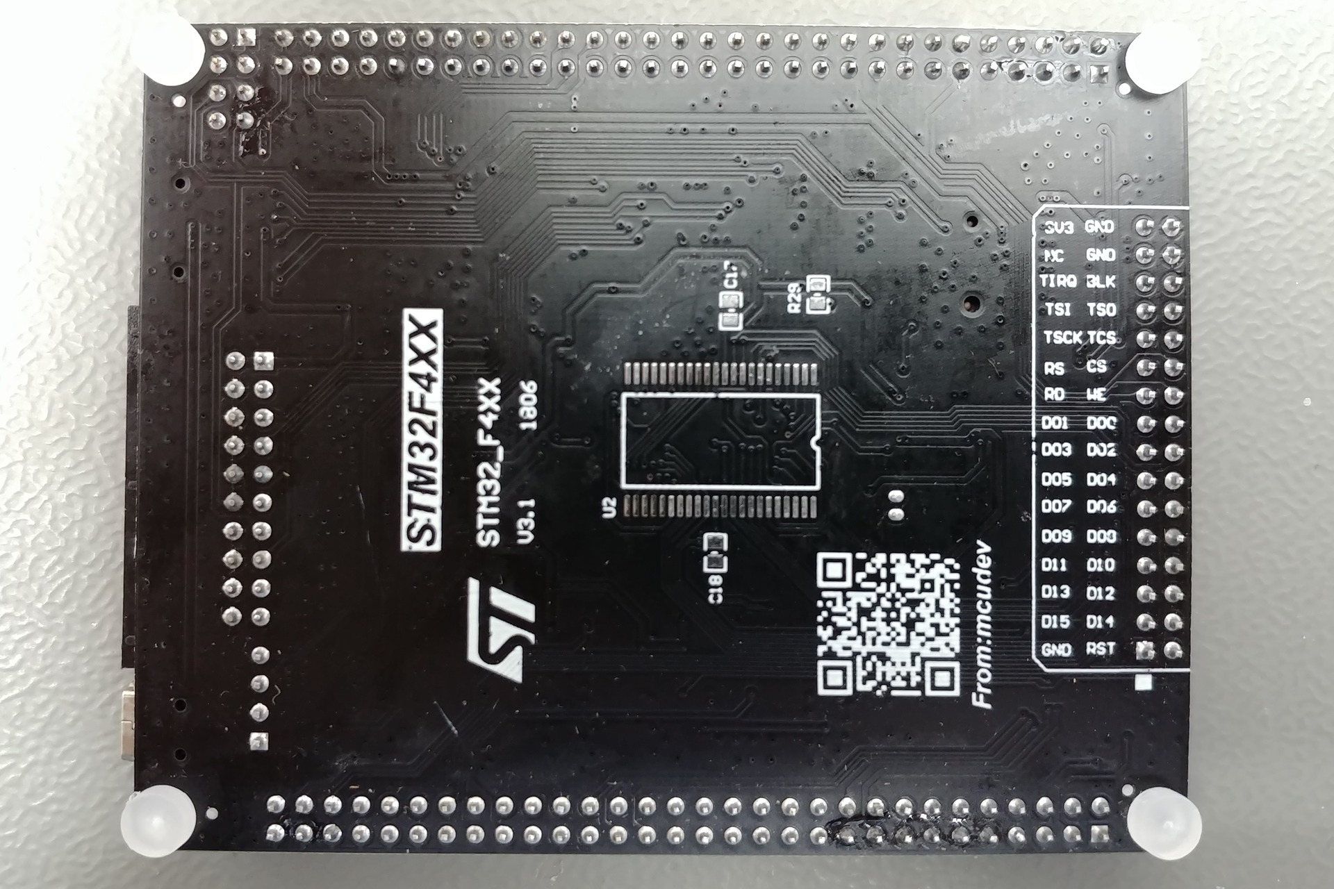
IS62WV51216 properties footprint
| Name | Unknown |
| Reference | U2 |
| Manufacturer | Integrated Silicon Solution, Inc. |
| Part | IS62WV51216 |
| Marking | IS62WV51216 |
| Datasheet | IS62WV51216.pdf |
| Package | TSOP - II 44 pins |
| Description | 8MiB SRAM |
IS62WV51216 pins footprint
| # | Name | Function | Connected to |
|---|---|---|---|
| 1 | - | A4 | PF4 |
| 2 | - | A3 | PF3 |
| 3 | - | A2 | PF2 |
| 4 | - | A1 | PF1 |
| 5 | - | A0 | PF0 |
| 6 | - | CS1 | PG10 |
| 7 | - | I/O0 | PD14 |
| 8 | - | I/O1 | PD15 |
| 9 | - | I/O2 | PD0 |
| 10 | - | I/O3 | PD1 |
| 11 | - | VDD | +3.3V rail |
| 12 | - | GND | Ground plane |
| 13 | - | I/O4 | PE7 |
| 14 | - | I/O5 | PE8 |
| 15 | - | I/O6 | PE9 |
| 16 | - | I/O7 | PE10 |
| 17 | - | WE | PD5 |
| 18 | - | A16 | PD11 |
| 19 | - | A15 | PG5 |
| 20 | - | A14 | PG4 |
| 21 | - | A13 | PG3 |
| 22 | - | A12 | PG2 |
| 23 | - | A17 | PD12 |
| 24 | - | A11 | PG1 |
| 25 | - | A10 | PG0 |
| 26 | - | A9 | PF15 |
| 27 | - | A8 | PF14 |
| 28 | - | A18 | PD13 |
| 29 | - | I/O8 | PE11 |
| 30 | - | I/O9 | PE12 |
| 31 | - | I/O10 | PE13 |
| 32 | - | I/O11 | PE14 |
| 33 | - | VDD | +3.3V rail |
| 34 | - | GND | Ground plane |
| 35 | - | I/O12 | PE15 |
| 36 | - | I/O13 | PD8 |
| 37 | - | I/O14 | PD9 |
| 38 | - | I/O15 | PD10 |
| 39 | - | LB | PE0 |
| 40 | - | UB | PE1 |
| 41 | - | OE | PD4 |
| 42 | - | A7 | PF13 |
| 43 | - | A6 | PF12 |
| 44 | - | A5 | PF5 |