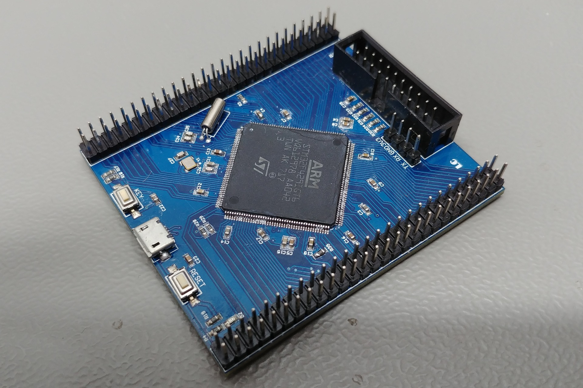
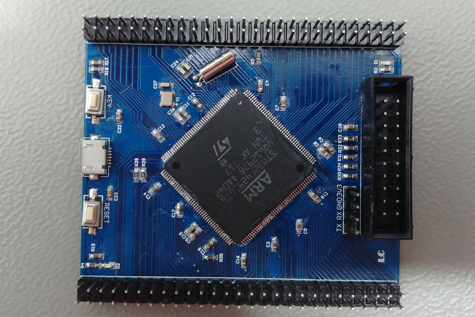
LC Technology STM32F429IGT6
STM32F429IGT6
Board
| Name | LC Technology STM32F429IGT6 |
| Part | STM32F429_F7 |
| Brand | Shenzhen LC Technology Co., Ltd. |
| Origin | China |
Microcontroller
| Part | STM32F429IGT6 |
| Manufacturer | ST-Microelectronics |
| Core | Arm Cortex-M4 |
| Max. Clock Speed | 180MHz |
| Package | LQFP 176 pins |
Internal memories
| FLASH | 1024KiB |
| SRAM | 256KiB |
| Backup SRAM | 4KiB |
Oscillators
| HSI | 16MHz |
| LSI | 32kHz |
| HSE | 25MHz |
| LSE | 32.768kHz |
Power
| Sources | Any +3.3V pin (+3.3V) Any +5V pin (+5V) USB connector (+5V) |
| VDDA pin | No |
| VSSA pin | No |
| VREF- pin | No |
| VREF+ pin | No |
| Backup battery | Pin |
Regulator
| Manufacturer | Advanced Monolithic Systems Inc. |
| Part | AMS1117 (AMS1117) |
| Package | SOT223 3 pins |
| Input | +4.6V to +15V |
| Output | +3.3V @ 1A |
| Datasheet | AMS1117.pdf |
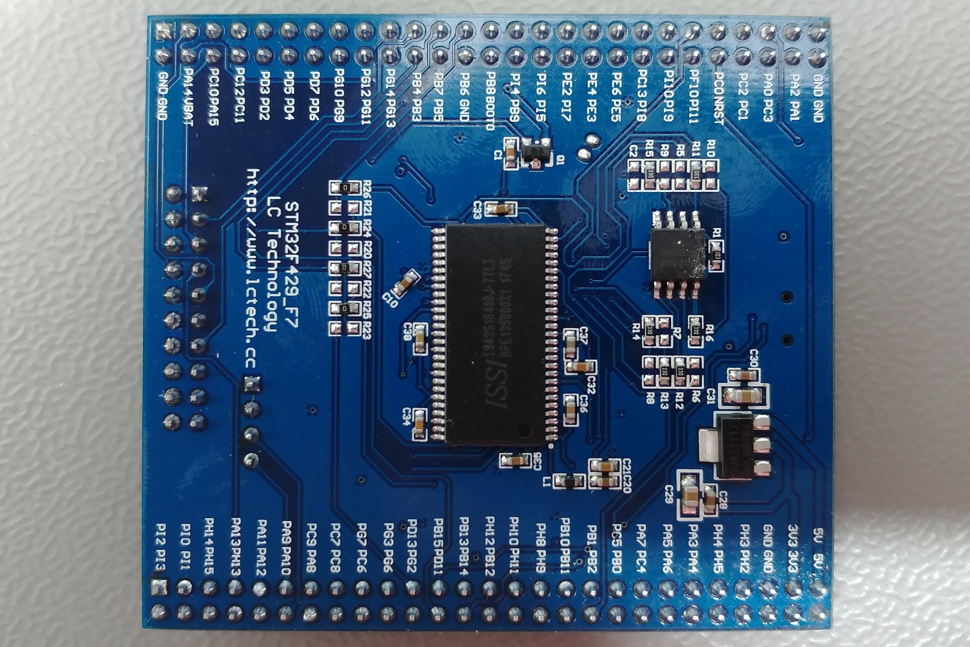
PCB
| Color | Blue |
| Size (w x l) | 62mm x 69mm |
| Mounting | None |
Remarks
- Warning: The +5V pins on this board are directly connected to the +5V pin of the USB connector. There is no protection in place. Do not power this board through USB and an external power supply at the same time.
Pictures
Resources
Inputs
Connectors
Devices
Inputs & outputs
Reset button
| Name | RESET |
| Reference | - |
| Type | Button |
| Connected to | NRST |
| Mode | Active low |
User button
| Name | KEY |
| Reference | - |
| Type | Button |
| Connected to | PA0 |
| Mode | Active high |
Power LED
| Name | - |
| Reference | D2 |
| Type | LED |
| Connected to | +3.3V rail |
| Mode | N.A. |
User LED
| Name | - |
| Reference | D1 |
| Type | LED |
| Connected to | PD12 |
| Mode | Sink |
Connectors & headers
Header 1 properties
| Name | Unknown |
| Reference | None |
| Type | Pin header (2.54mm, 27x2, male) |
Header 1 pins
| # | Name | Function | Connected to |
|---|---|---|---|
| 1 | GND | - | Ground plane |
| 2 | GND | - | Ground plane |
| 3 | PA14 | - | PA14 |
| 4 | VBAT | - | VBAT |
| 5 | PC10 | - | PC10 |
| 6 | PA15 | - | PA15 |
| 7 | PC12 | - | PC12 |
| 8 | PC11 | - | PC11 |
| 9 | PD3 | - | PD3 |
| 10 | PD2 | - | PD2 |
| 11 | PD5 | - | PD5 |
| 12 | PD4 | - | PD4 |
| 13 | PD7 | - | PD7 |
| 14 | PD6 | - | PD6 |
| 15 | PG10 | - | PG10 |
| 16 | PG9 | - | PG9 |
| 17 | PG12 | - | PG12 |
| 18 | PG11 | - | PG11 |
| 19 | PG14 | - | PG14 |
| 20 | PG13 | - | PG13 |
| 21 | PB4 | - | PB4 |
| 22 | PB3 | - | PB3 |
| 23 | PB7 | - | PB7 |
| 24 | PB5 | - | PB5 |
| 25 | PB6 | - | PB6 |
| 26 | GND | - | Ground plane |
| 27 | PB8 | - | PB8 |
| 28 | BOOT0 | - | BOOT0 |
| 29 | PI4 | - | PI4 |
| 30 | PB9 | - | PB9 |
| 31 | PI6 | - | PI6 |
| 32 | PI5 | - | PI5 |
| 33 | PE2 | - | PE2 |
| 34 | PI7 | - | PI7 |
| 35 | PE4 | - | PE4 |
| 36 | PE3 | - | PE3 |
| 37 | PE6 | - | PE6 |
| 38 | PE5 | - | PE5 |
| 39 | PC13 | - | PC13 |
| 40 | PI8 | - | PI8 |
| 41 | PI10 | - | PI10 |
| 42 | PI9 | - | PI9 |
| 43 | PF10 | - | PF10 |
| 44 | PI11 | - | PI11 |
| 45 | PC0 | - | PC0 |
| 46 | NRST | - | NRST |
| 47 | PC2 | - | PC2 |
| 48 | PC1 | - | PC1 |
| 49 | PA0 | - | PA0 |
| 50 | PC3 | - | PC3 |
| 51 | PA2 | - | PA2 |
| 52 | PA1 | - | PA1 |
| 53 | GND | - | Ground plane |
| 54 | GND | - | Ground plane |
Header 2 properties
| Name | Unknown |
| Reference | None |
| Type | Pin header (2.54mm, 27x2, male) |
Header 2 pins
| # | Name | Function | Connected to |
|---|---|---|---|
| 1 | PI2 | - | PI2 |
| 2 | PI3 | - | PI3 |
| 3 | PI0 | - | PI0 |
| 4 | PI1 | - | PI1 |
| 5 | PH14 | - | PH14 |
| 6 | PH15 | - | PH15 |
| 7 | PA13 | - | PA13 |
| 8 | PH13 | - | PH13 |
| 9 | PA11 | - | PA11 |
| 10 | PA12 | - | PA12 |
| 11 | PA9 | - | PA9 |
| 12 | PA10 | - | PA10 |
| 13 | PC9 | - | PC9 |
| 14 | PA8 | - | PA8 |
| 15 | PC7 | - | PC7 |
| 16 | PC8 | - | PC8 |
| 17 | PG7 | - | PG7 |
| 18 | PC6 | - | PC6 |
| 19 | PG3 | - | PG3 |
| 20 | PG6 | - | PG6 |
| 21 | PD13 | - | PD13 |
| 22 | PG2 | - | PG2 |
| 23 | PB15 | - | PB15 |
| 24 | PD11 | - | PD11 |
| 25 | PB13 | - | PB13 |
| 26 | PB14 | - | PB14 |
| 27 | PH12 | - | PH12 |
| 28 | PB12 | - | PB12 |
| 29 | PH10 | - | PH10 |
| 30 | PH11 | - | PH11 |
| 31 | PH8 | - | PH8 |
| 32 | PH9 | - | PH9 |
| 33 | PB10 | - | PB10 |
| 34 | PB11 | - | PB11 |
| 35 | PB1 | - | PB1 |
| 36 | PB2 | - | PB2 |
| 37 | PC5 | - | PC5 |
| 38 | PB0 | - | PB0 |
| 39 | PA7 | - | PA7 |
| 40 | PC4 | - | PC4 |
| 41 | PA5 | - | PA5 |
| 42 | PA6 | - | PA6 |
| 43 | PA3 | - | PA3 |
| 44 | PA4 | - | PA4 |
| 45 | PH4 | - | PH4 |
| 46 | PH5 | - | PH5 |
| 47 | PH3 | - | PH3 |
| 48 | PH2 | - | PH2 |
| 49 | GND | - | Ground plane |
| 50 | GND | - | Ground plane |
| 51 | 3V3 | - | +3.3V rail |
| 52 | 3V3 | - | +3.3V rail |
| 53 | 5V | - | +5V rail |
| 54 | 5V | - | +5V rail |
USB connector properties
| Name | Unknown |
| Reference | None |
| Type | USB Mini |
USB connector pins
| # | Name | Function | Connected to |
|---|---|---|---|
| 1 | - | VCC | +5V rail |
| 2 | - | D- | PB14 |
| 3 | - | D+ | PB15 |
| 4 | - | ID | N.C. |
| 5 | - | GND | Ground plane |
JTAG header properties
| Name | Unknown |
| Reference | None |
| Type | IDC (2.54mm, 10x2, male) |
JTAG header pins
| # | Name | Function | Connected to |
|---|---|---|---|
| 1 | - | VCC | +3.3V rail |
| 2 | - | VCC | +3.3V rail |
| 3 | - | TRST | PB4 |
| 4 | - | GND | Ground plane |
| 5 | - | TDI | PA15 |
| 6 | - | GND | Ground plane |
| 7 | - | TMS / SWDIO | PA13 |
| 8 | - | GND | Ground plane |
| 9 | - | TCLK / SWCLK | PA14 |
| 10 | - | GND | Ground plane |
| 11 | - | RTCK | N.C. |
| 12 | - | GND | Ground plane |
| 13 | - | TDO / SWO | PB3 |
| 14 | - | GND | Ground plane |
| 15 | - | RESET | NRST |
| 16 | - | GND | Ground plane |
| 17 | - | N.C. | N.C. |
| 18 | - | GND | Ground plane |
| 19 | - | N.C. | N.C. |
| 20 | - | GND | Ground plane |
Serial header properties
| Name | Unknown |
| Reference | None |
| Type | Pin header (2.54mm, 4x1, male) |
Serial header pins
| # | Name | Function | Connected to |
|---|---|---|---|
| 1 | 3V3 | - | +3.3V rail |
| 2 | GND | - | Ground plane |
| 3 | RX | - | PA10 |
| 4 | TX | - | PA9 |
Devices
IS42S16400J properties
| Name | Unknown |
| Reference | Unknown |
| Manufacturer | Integrated Silicon Solution, Inc. |
| Part | IS42S16400J |
| Marking | IS42S16400J-71L |
| Datasheet | IS42S16400J.pdf |
| Package | TSOP - II 54 pins |
| Description | 8MiB SDRAM |
IS42S16400J pins
| # | Name | Function | Connected to |
|---|---|---|---|
| 1 | - | VDD | +3.3V rail |
| 2 | - | DQ0 | PD14 |
| 3 | - | VDDQ | +3.3V rail |
| 4 | - | DQ1 | PD15 |
| 5 | - | DQ2 | PD0 |
| 6 | - | GNDQ | Ground plane |
| 7 | - | DQ3 | PD1 |
| 8 | - | DQ4 | PE7 |
| 9 | - | VDDQ | +3.3V rail |
| 10 | - | DQ5 | PE8 |
| 11 | - | DQ6 | PE9 |
| 12 | - | GNDQ | Ground plane |
| 13 | - | DQ7 | PE10 |
| 14 | - | VDD | +3.3V rail |
| 15 | - | LDQM | PE0 |
| 16 | - | WE | PH5 |
| 17 | - | CAS | PG15 |
| 18 | - | RAS | PF11 |
| 19 | - | CS | PH6 |
| 20 | - | BA0 | PG4 |
| 21 | - | BA1 | PG5 |
| 22 | - | A10 | PG0 |
| 23 | - | A0 | PF0 |
| 24 | - | A1 | PF1 |
| 25 | - | A2 | PF2 |
| 26 | - | A3 | PF3 |
| 27 | - | VDD | +3.3V rail |
| 28 | - | GND | Ground plane |
| 29 | - | A4 | PF4 |
| 30 | - | A5 | PF5 |
| 31 | - | A6 | PF12 |
| 32 | - | A7 | PF13 |
| 33 | - | A8 | PF14 |
| 34 | - | A9 | PF15 |
| 35 | - | A11 | PG1 |
| 36 | - | NC | N.C. |
| 37 | - | CKE | PH7 |
| 38 | - | CLK | PG8 |
| 39 | - | UDQM | PE1 |
| 40 | - | NC | N.C. |
| 41 | - | GND | Ground plane |
| 42 | - | DQ8 | PE11 |
| 43 | - | VDDQ | +3.3V rail |
| 44 | - | DQ9 | PE12 |
| 45 | - | DQ10 | PE13 |
| 46 | - | GNDQ | Ground plane |
| 47 | - | DQ11 | PE14 |
| 48 | - | DQ12 | PE15 |
| 49 | - | VDDQ | +3.3V rail |
| 50 | - | DQ13 | PD8 |
| 51 | - | DQ14 | PD9 |
| 52 | - | GNDQ | Ground plane |
| 53 | - | DQ15 | PD10 |
| 54 | - | GND | Ground plane |
W25Q128FV properties
| Name | Unknown |
| Reference | Unknown |
| Manufacturer | Winbond Electronics Corporation |
| Part | W25Q128FV |
| Marking | W25Q128FVSG |
| Datasheet | W25Q128FV.pdf |
| Package | SOIC 8 pins |
| Description | 16MiB Dual/Quad SPI FLASH |
W25Q128FV pins
| # | Name | Function | Connected to |
|---|---|---|---|
| 1 | - | /CS | PF6 via 330Ω resistor, pulled down up by 10kΩ resistor |
| 2 | - | DO | PF9 via 330Ω resistor |
| 3 | - | /WP | N.C. |
| 4 | - | GND | Ground plane |
| 5 | - | DI | PF8 via 330Ω resistor |
| 6 | - | CLK | PF7 via 330Ω resistor |
| 7 | - | /HOLD | +3.3V rail |
| 8 | - | VCC | +3.3V rail via 330Ω resistor |