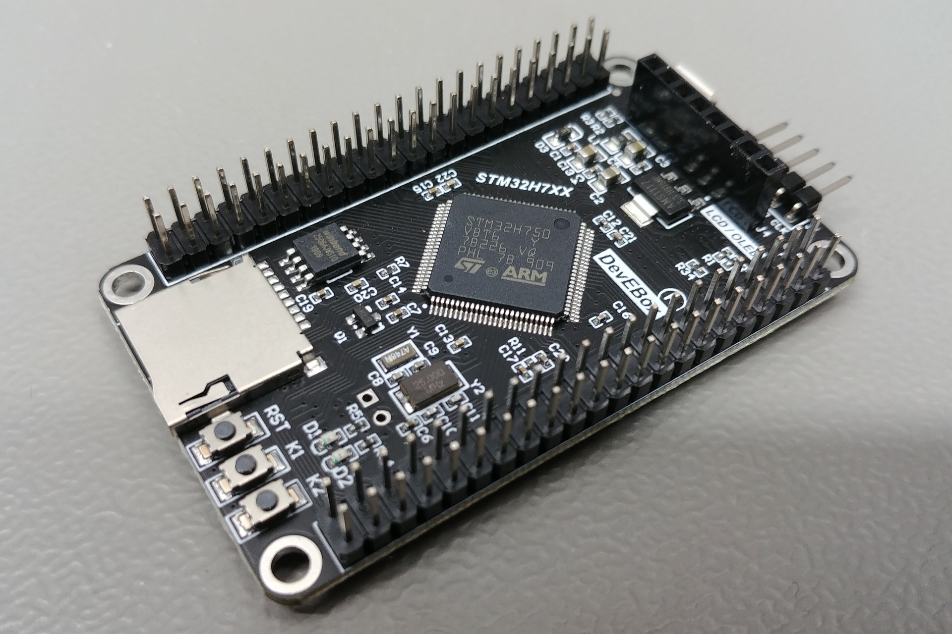
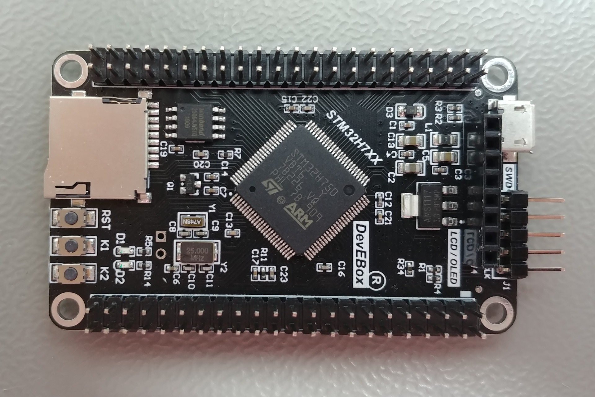
STM32H7XX M
STM32H750VBT6
Board
| Name | STM32H7XX M |
| Part | STM32F7XX_M (note the typo F instead of H) |
| Brand | DevEBox |
| Origin | China |
Microcontroller
| Part | STM32H750VBT6 |
| Manufacturer | ST-Microelectronics |
| Core | Arm Cortex-M7 |
| Max. Clock Speed | 400MHz |
| Package | UFQFPN 100 pins |
Internal memories
| FLASH | 128KiB |
| SRAM | 1024KiB |
Oscillators
| HSI | 64MHz |
| LSI | 32kHz |
| HSE | 25MHz |
| LSE | 32.768kHz |
Power
| Sources | Any +3.3V pin (+3.3V) Any +5V pin (+5V) USB connector (+5V) |
| VDDA pin | Yes |
| VSSA pin | No |
| VREF- pin | No |
| VREF+ pin | Yes |
| Backup battery | Header |
Regulator
| Manufacturer | Advanced Monolithic Systems Inc. |
| Part | AMS1117 (AMS1117) |
| Package | SOT223 3 pins |
| Input | +4.6V to +15V |
| Output | +3.3V @ 1A |
| Datasheet | AMS1117.pdf |
PCB
| Color | Black |
| Size (w x l) | 40mm x 68mm |
| Mounting | 4x mounting hole (M3) |
Remarks
- Warning: The +5V pins on this board are directly connected to the +5V pin of the USB connector. There is no protection in place. Do not power this board through USB and an external power supply at the same time.
Pictures
Resources
Devices
Inputs & outputs
Reset button
| Name | RST |
| Reference | - |
| Type | Button |
| Connected to | NRST |
| Mode | Active low |
User button 1
| Name | K1 |
| Reference | - |
| Type | Button |
| Connected to | PE3 |
| Mode | Active low |
User button 2
| Name | K2 |
| Reference | - |
| Type | Button |
| Connected to | PC5 |
| Mode | Active low |
Power LED
| Name | D1 |
| Reference | - |
| Type | LED |
| Connected to | +3.3V rail |
| Mode | N.A. |
User LED
| Name | D2 |
| Reference | - |
| Type | LED |
| Connected to | PA1 |
| Mode | Sink |
Connectors & headers
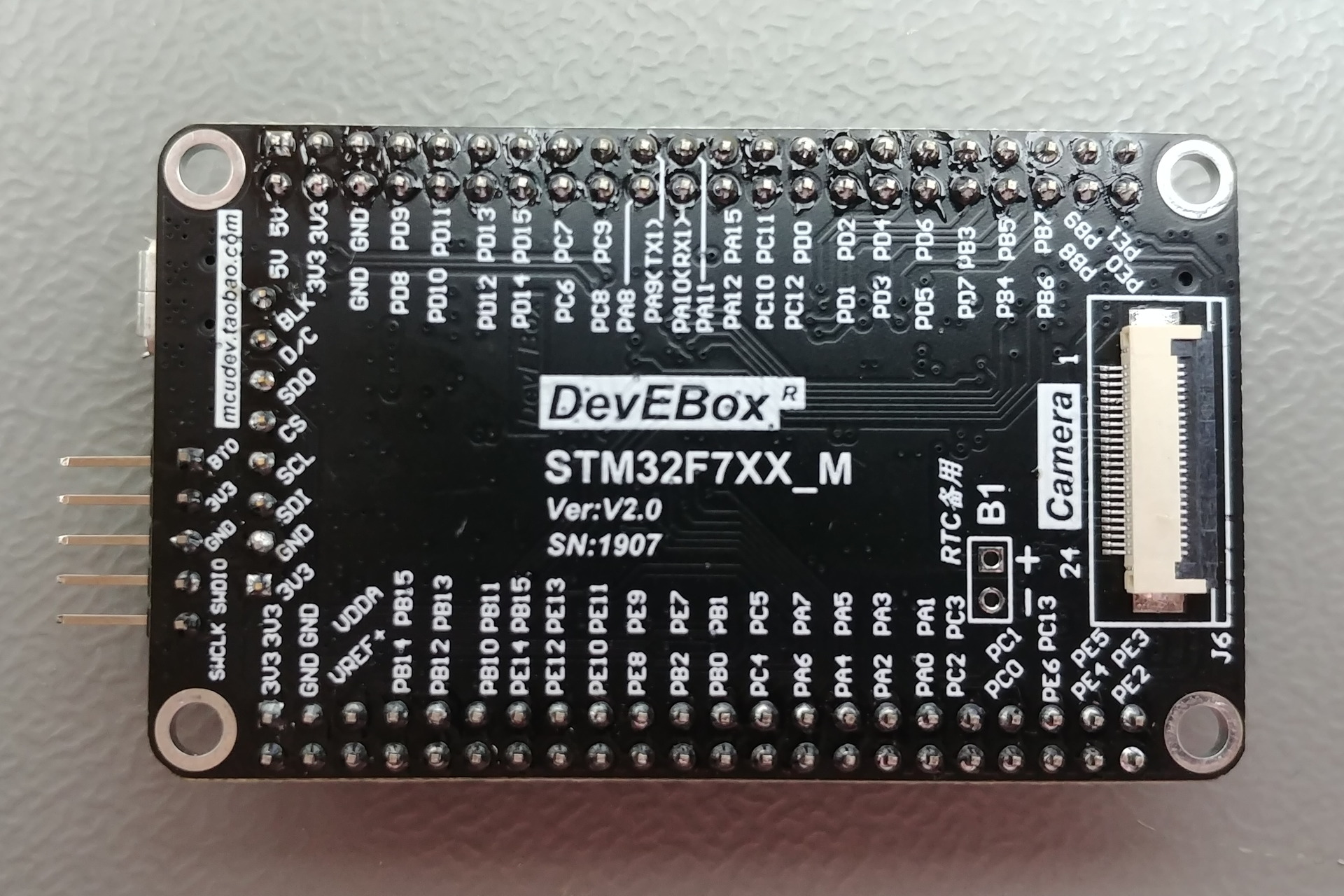
Header 1 properties
| Name | Unknown |
| Reference | None |
| Type | Pin header (2.54mm, 22x2, male) |
Header 1 pins
| # | Name | Function | Connected to |
|---|---|---|---|
| 1 | 3V3 | - | +3.3V rail |
| 2 | 3V3 | - | +3.3V rail |
| 3 | GND | - | Ground plane |
| 4 | GND | - | Ground plane |
| 5 | VDDA | - | VDDA |
| 6 | VREF+ | - | VREF+ |
| 7 | PB15 | - | PB15 |
| 8 | PB14 | - | PB14 |
| 9 | PB13 | - | PB13 |
| 10 | PB12 | - | PB12 |
| 11 | PB11 | - | PB11 |
| 12 | PB10 | - | PB10 |
| 13 | PE15 | - | PE15 |
| 14 | PE14 | - | PE14 |
| 15 | PE13 | - | PE13 |
| 16 | PE12 | - | PE12 |
| 17 | PE11 | - | PE11 |
| 18 | PE10 | - | PE10 |
| 19 | PE9 | - | PE9 |
| 20 | PE8 | - | PE8 |
| 21 | PE7 | - | PE7 |
| 22 | PB2 | - | PB2 |
| 23 | PB1 | - | PB1 |
| 24 | PB0 | - | PB0 |
| 25 | PC5 | - | PC5 |
| 26 | PC4 | - | PC4 |
| 27 | PA7 | - | PA7 |
| 28 | PA6 | - | PA6 |
| 29 | PA5 | - | PA5 |
| 30 | PA4 | - | PA4 |
| 31 | PA3 | - | PA3 |
| 32 | PA2 | - | PA2 |
| 33 | PA1 | - | PA1 |
| 34 | PA0 | - | PA0 |
| 35 | PC3 | - | PC3 |
| 36 | PC2 | - | PC2 |
| 37 | PC1 | - | PC1 |
| 38 | PC0 | - | PC0 |
| 39 | PC13 | - | PC13 |
| 40 | PE6 | - | PE6 |
| 41 | PE5 | - | PE5 |
| 42 | PE4 | - | PE4 |
| 43 | PE3 | - | PE3 |
| 44 | PE2 | - | PE2 |
Header 2 properties
| Name | Unknown |
| Reference | None |
| Type | Pin header (2.54mm, 22x2, male) |
Header 2 pins
| # | Name | Function | Connected to |
|---|---|---|---|
| 1 | 5V | - | +5V rail |
| 2 | 5V | - | +5V rail |
| 3 | 3V3 | - | +3.3V rail |
| 4 | 3V3 | - | +3.3V rail |
| 5 | GND | - | Ground plane |
| 6 | GND | - | Ground plane |
| 7 | PD9 | - | PD9 |
| 8 | PD8 | - | PD8 |
| 9 | PD11 | - | PD11 |
| 10 | PD10 | - | PD10 |
| 11 | PD13 | - | PD13 |
| 12 | PD12 | - | PD12 |
| 13 | PD15 | - | PD15 |
| 14 | PD14 | - | PD14 |
| 15 | PC7 | - | PC7 |
| 16 | PC6 | - | PC6 |
| 17 | PC9 | - | PC9 |
| 18 | PC8 | - | PC8 |
| 19 | PA9(TX1) | - | PA9 |
| 20 | PA8 | - | PA8 |
| 21 | PA11 | - | PA11 |
| 22 | PA10(RX1) | - | PA10 |
| 23 | PA15 | - | PA15 |
| 24 | PA12 | - | PA12 |
| 25 | PC11 | - | PC11 |
| 26 | PC10 | - | PC10 |
| 27 | PD0 | - | PD0 |
| 28 | PC12 | - | PC12 |
| 29 | PD2 | - | PD2 |
| 30 | PD1 | - | PD1 |
| 31 | PD4 | - | PD4 |
| 32 | PD3 | - | PD3 |
| 33 | PD6 | - | PD6 |
| 34 | PD5 | - | PD5 |
| 35 | PB3 | - | PB3 |
| 36 | PD7 | - | PD7 |
| 37 | PB5 | - | PB5 |
| 38 | PB4 | - | PB4 |
| 39 | PB7 | - | PB7 |
| 40 | PB6 | - | PB6 |
| 41 | PB9 | - | PB9 |
| 42 | PB8 | - | PB8 |
| 43 | PE1 | - | PE1 |
| 44 | PE0 | - | PE0 |
USB connector properties
| Name | Unknown |
| Reference | J5 |
| Type | USB Micro |
USB connector pins
| # | Name | Function | Connected to |
|---|---|---|---|
| 1 | - | VCC | +5V rail |
| 2 | - | D- | PA11 via 22Ω resistor (R2) |
| 3 | - | D+ | PA12 via 22Ω resistor (R3) |
| 4 | - | ID | N.C. |
| 5 | - | GND | Ground plane |
SWD header properties
| Name | SWD |
| Reference | J1 |
| Type | Pin header (2.54mm, 22x2, male) |
SWD header pins
| # | Name | Function | Connected to |
|---|---|---|---|
| 1 | BT0 | - | BOOT0 |
| 2 | 3V3 | - | +3.3V rail |
| 3 | GND | - | Ground plane |
| 4 | SWDIO | - | PA13 |
| 5 | SWCLK | - | PA14 |
TFT header properties
| Name | LCD / OLED |
| Reference | J4 |
| Type | Pin header (2.54mm, 8x1, female) |
TFT header pins
| # | Name | Function | Connected to |
|---|---|---|---|
| 1 | 3V3 | - | +3.3V rail |
| 2 | GND | - | Ground plane |
| 3 | SDI | - | PB15 |
| 4 | SCL | - | PB13 |
| 5 | CS | - | PB12 |
| 6 | SDO | - | PB14 |
| 7 | D/C | - | PB1 |
| 8 | BLK | - | PB0 |
SD-card connector properties
| Name | Unknown |
| Reference | None |
| Type | microSD |
SD-card connector pins
| # | Name | Function | Connected to |
|---|---|---|---|
| 1 | - | DAT2 | PC10 |
| 2 | - | CD/DAT3 | PC11 |
| 3 | - | CMD | PD2 |
| 4 | - | VDD | +3.3V rail |
| 5 | - | CLK | PC12 |
| 6 | - | VSS | Ground plane |
| 7 | - | DAT0 | PC8 |
| 8 | - | DAT1 | PC9 |
| 9 | - | CD | N.C. |
| 10 | - | Body | Ground plane |
Battery header properties footprint
| Name | Unknown |
| Reference | B1 |
| Type | Pin header (2.54mm, 2x1, male) |
Battery header pins footprint
| # | Name | Function | Connected to |
|---|---|---|---|
| 1 | + | - | VBAT |
| 2 | - | - | Ground plane |
Devices
W25Q64JV properties
| Name | Unknown |
| Reference | Unknown |
| Manufacturer | Winbond Electronics Corporation |
| Part | W25Q64JV |
| Marking | W25Q64JVSIQ |
| Datasheet | W25Q64JV.pdf |
| Package | SOIC 8 pins |
| Description | 8MiB Dual/Quad SPI FLASH |
W25Q64JV pins
| # | Name | Function | Connected to |
|---|---|---|---|
| 1 | - | /CS | PB6 |
| 2 | - | DO | PD12 |
| 3 | - | IO2 | PE2 |
| 4 | - | GND | Ground plane |
| 5 | - | DI | PD11 |
| 6 | - | CLK | PB2 |
| 7 | - | IO3 | PD13 |
| 8 | - | VCC | +3.3V rail |