Guide: Connecting your debugger
This small guide will explain how to connect your debugger to your development board. There are two commonly used connectors which expose only the SWD (Serial Wire Debug) interface or the full JTAG interface.
Connecting ST’s Nucleo and Discovery boards
If you are using one of ST’s official Nucleo or Discovery boards, you do not have to connect an external debugger. These board come with an on-board ST-LINK/V2 debugger. Just connect the board via USB to your PC and you are ready to go!
Connecting Chinese development boards
If you are using one of the many Chinese development boards, you most likely need to connect an external debugger to flash and debug the device on your development board as these board normally do not include a on-board ST-LINK/V2.
Connecting via SWD header
The easiest way to connect your development board to your debugger is by using the 4-pin SWD header, if present. This header is usually a male dupont header, but female headers are also used. The header exposes a ground pin, a +3.3V pin, a clock pin, and a data pin.
Note: There is no particular order in which these pins are arranged.
Warning: Do not connect the +3.3V pin if you are powering your board externally, as most Chinese development boards do not have any protection on the power pins. This may cause damage your board, debugger or PC.
The table below provides an overview of which pins to connect:
| Pin function | Debugger pin | Target pin |
|---|---|---|
| Ground pin | GND |
GND |
| +3.3V pin | VCC / VDD / 3.3V |
VCC / VDD / 3.3V |
| Clock pin | SWCLK / SWCK |
CLK / SWCLK |
| Data pin | SWDIO |
DIO / SWDIO |
Connecting to JTAG header
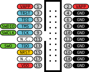
If your development board does not have a 4-pin SWD header, it most likely does have a 20-pin JTAG header. This connector exposes all the pins needed for full JTAG support. This includes the pins a SWD header would expose. Refer to the image below for an overview of a typical ARM JTAG header.
Warning: Do not connect the +3.3V pin if you are powering your board externally, as most Chinese development boards do not have any protection on the power pins. This may cause damage your board, debugger or PC.
The table below provides an overview of which pins to connect:
| Pin function | Debugger pin | Target pin |
|---|---|---|
| Ground pin | GND |
GND |
| +3.3V pin | VCC / VDD / 3.3V |
VCC |
| Clock pin | SWCLK / SWCK |
SWCLK |
| Data pin | SWDIO |
SWDIO |
Connecting to GPIO pins
If you have a development board that does not have a SWD or JTAG header, you can also connect your debugger to some specific GPIO ports. This is essentially the same as connecting your debugger via a SWD or JTAG header, although a bit more cumbersome.
Warning: Do not connect the +3.3V pin if you are powering your board externally, as most Chinese development boards do not have any protection on the power pins. This may cause damage your board, debugger or PC.
The table below provides an overview of which pins to connect:
| Pin function | Debugger pin | Target pin |
|---|---|---|
| Ground pin | GND |
Any GND pin |
| +3.3V pin | VCC / VDD / 3.3V |
Any +3.3V pin |
| Clock pin | SWCLK / SWCK |
PA14 |
| Data pin | SWDIO |
PA13 |
Debuggers
There are a few different debuggers that can be used.
Official ST-LINK/V2
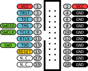
The official ST-LINK/V2 is a debugger manufactured by ST Microelectronics and can be bought at any major electronics distributor. In addition to the standard ST-LINK/V2, ST offers a ST-LINK/V2-ISOL variant which features digital isolation between the PC and target board. This isolation withstands voltages up to 1000Vrms.
This debugger has a 20-pin IDC conenctor for connecting to target boards. The pinout of this connector can be found below.
Nucleo ST-LINK/V2
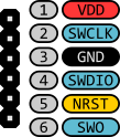
The ST-LINK/V2 built into the Nucleo-64 and Nucleo-144 boards can also be used as stand-alone debugger. To use the built-in debugger, you must remove the jumpers from CN2 (Nucleo-64) or CN4 (Nucleo-144). Then you can use CN4 (Nucleo-64) or CN6 (Nucleo-144) to connect to your target board.
This debugger has a 6-pin dupont header for connecting to a SWD header on the target board. The pinout of this connector can be found below.
ST-LINK/V2 Clone
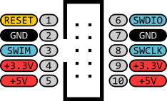
The cheapest alternative to both official ST options is a Chinese ST-LINK/V2 clone. This clone offers the same connectivity when it comes to SWD. It does not expose a full JTAG interface. However, it does feature some additional power pins, both +5V and +3.3V.
This debugger has a 10-pin IDC connector. The pinout of this connector can be found below.