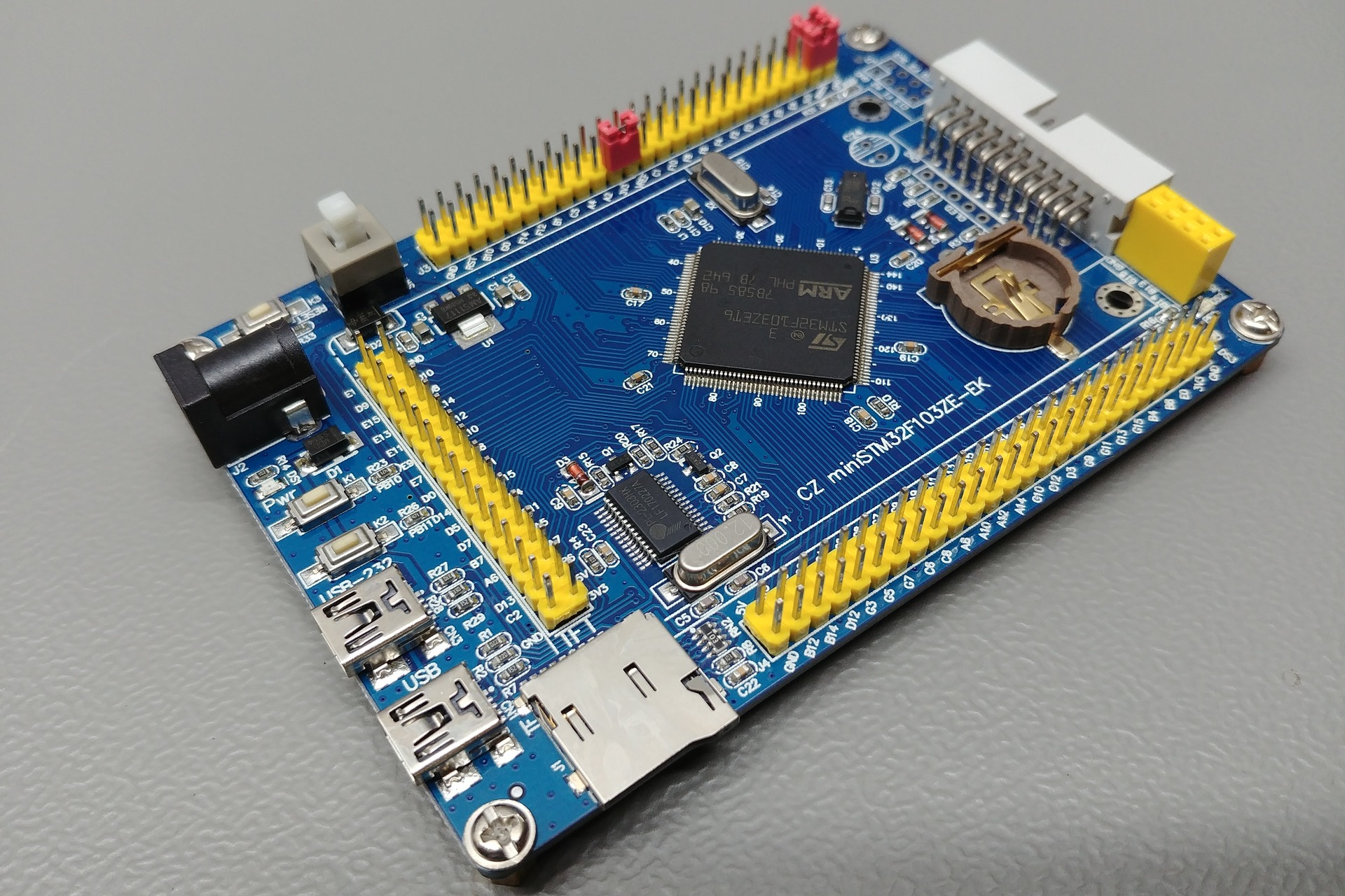
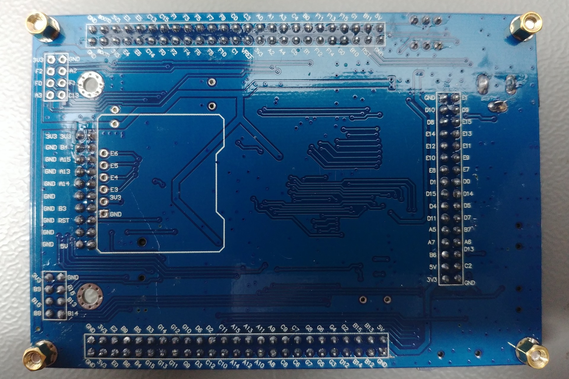
CZ miniSTM32F103ZE-EK
STM32F103ZET6
Board
| Name | CZ miniSTM32F103ZE-EK |
| Part | Unknown |
| Brand | Unknown |
| Origin | China |
Microcontroller
| Part | STM32F103ZET6 |
| Manufacturer | ST-Microelectronics |
| Core | Arm Cortex-M3 |
| Max. Clock Speed | 72MHz |
| Package | LQFP 144 pins |
Internal memories
| FLASH | 512KiB |
| SRAM | 64KiB |
Oscillators
| HSI | 8MHz |
| LSI | 40kHz |
| HSE | 8MHz |
| LSE | 32.768kHz |
Power
| Sources | Any +3.3V pin (+3.3V) Any +5V pin (+5V) USB connector (+5V) |
| VDDA pin | No |
| VSSA pin | No |
| VREF- pin | No |
| VREF+ pin | Yes |
| Backup battery | Holder (12.5mm / 12) |
Regulator
| Manufacturer | Advanced Monolithic Systems Inc. |
| Part | AMS1117 (AMS1117) |
| Package | SOT223 3 pins |
| Input | +4.6V to +15V |
| Output | +3.3V @ 1A |
| Datasheet | AMS1117.pdf |
PCB
| Color | Blue |
| Size (w x l) | 65mm x 108mm |
| Mounting | 4x mounting hole (M3) |
Remarks
- Warning: The +5V pins on this board are directly connected to the +5V pin of the USB connector. There is no protection in place. Do not power this board through USB and an external power supply at the same time.
Pictures
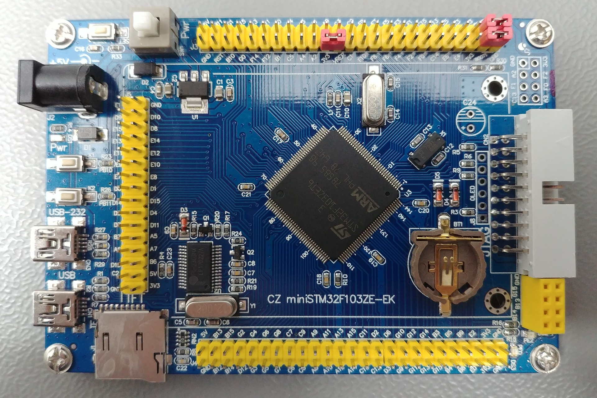
Outputs
Devices
Inputs & outputs
Reset button
| Name | RESET |
| Reference | K3 |
| Type | Button |
| Connected to | NRST |
| Mode | Active low |
BOOT0 jumper
| Name | - |
| Reference | - |
| Type | 2-way jumper |
| Connected to | BOOT0 |
| Mode | N.A. |
- Note: This jumper is part of Header 1.
BOOT1 jumper
| Name | - |
| Reference | - |
| Type | 2-way jumper |
| Connected to | PB2 |
| Mode | N.A. |
- Note: This jumper is part of Header 1.
User button 1
| Name | - |
| Reference | K1 |
| Type | Button |
| Connected to | PB10 |
| Mode | Active low |
User button 2
| Name | - |
| Reference | K2 |
| Type | Button |
| Connected to | PB11 |
| Mode | Active low |
Power source switch
| Name | Pwr |
| Reference | SW1 |
| Type | Switch |
| Connected to | +5V USB |
| Mode | N.A. |
Power LED
| Name | Pwr |
| Reference | DS1 |
| Type | LED |
| Connected to | +3.3V rail |
| Mode | N.A. |
User LED 1
| Name | - |
| Reference | DS2 |
| Type | LED |
| Connected to | PE2 |
| Mode | Sink |
User LED 2
| Name | - |
| Reference | DS3 |
| Type | LED |
| Connected to | PE0 |
| Mode | Sink |
Connectors & headers
Header 1 properties
| Name | Unknown |
| Reference | J3 |
| Type | Pin header (2.54mm, 25x2, male) |
Header 1 pins
| # | Name | Function | Connected to |
|---|---|---|---|
| 1 | GND | - | Ground plane |
| 2 | 5V | - | +5V rail |
| 3 | RST | - | NRST |
| 4 | B11 | - | PB11 |
| 5 | B10 | - | PB10 |
| 6 | G1 | - | PG1 |
| 7 | G0 | - | PG0 |
| 8 | F15 | - | PF15 |
| 9 | F14 | - | PF14 |
| 10 | F13 | - | PF13 |
| 11 | F12 | - | PF12 |
| 12 | F11 | - | PF11 |
| 13 | B1 | - | PB1 |
| 14 | B0 | - | PB0 |
| 15 | C5 | - | PC5 |
| 16 | C4 | - | PC4 |
| 17 | A4 | - | PA4 |
| 18 | A3 | - | PA3 |
| 19 | A2 | - | PA2 |
| 20 | A1 | - | PA1 |
| 21 | 3V3 | - | +3.3V rail |
| 22 | A0 | - | PA0 |
| 23 | VREF | - | VREF+ |
| 24 | C3 | - | PC3 |
| 25 | C1 | - | PC1 |
| 26 | C0 | - | PC0 |
| 27 | F10 | - | PF10 |
| 28 | F9 | - | PF9 |
| 29 | F8 | - | PF8 |
| 30 | F7 | - | PF7 |
| 31 | F6 | - | PF6 |
| 32 | F5 | - | PF5 |
| 33 | F4 | - | PF4 |
| 34 | F3 | - | PF3 |
| 35 | F2 | - | PF2 |
| 36 | F1 | - | PF1 |
| 37 | F0 | - | PF0 |
| 38 | C15 | - | PC15 |
| 39 | C14 | - | PC14 |
| 40 | C13 | - | PC13 |
| 41 | E6 | - | PE6 |
| 42 | E5 | - | PE5 |
| 43 | E4 | - | PE4 |
| 44 | D3 | - | PD3 |
| 45 | 3V3 | - | +3.3V rail |
| 46 | 3V3 | - | +3.3V rail |
| 47 | BOOT1 | - | PB2 |
| 48 | BOOT0 | - | BOOT0 |
| 49 | GND | - | Ground plane |
| 50 | GND | - | Ground plane |
Header 2 properties
| Name | Unknown |
| Reference | J4 |
| Type | Pin header (2.54mm, 25x2, male) |
Header 2 pins
| # | Name | Function | Connected to |
|---|---|---|---|
| 1 | GND | - | Ground plane |
| 2 | 5V | - | +5V rail |
| 3 | B12 | - | PB12 |
| 4 | B13 | - | PB13 |
| 5 | B14 | - | PB14 |
| 6 | B15 | - | PB15 |
| 7 | D12 | - | PD12 |
| 8 | G2 | - | PG2 |
| 9 | G3 | - | PG3 |
| 10 | G4 | - | PG4 |
| 11 | G5 | - | PG5 |
| 12 | G6 | - | PG6 |
| 13 | G7 | - | PG7 |
| 14 | G8 | - | PG8 |
| 15 | C6 | - | PC6 |
| 16 | C7 | - | PC7 |
| 17 | C8 | - | PC8 |
| 18 | C9 | - | PC9 |
| 19 | A8 | - | PA8 |
| 20 | A9 | - | PA9 |
| 21 | A10 | - | PA10 |
| 22 | A11 | - | PA11 |
| 23 | A12 | - | PA12 |
| 24 | A13 | - | PA13 |
| 25 | A14 | - | PA14 |
| 26 | A15 | - | PA15 |
| 27 | C10 | - | PC10 |
| 28 | C11 | - | PC11 |
| 29 | C12 | - | PC12 |
| 30 | D2 | - | PD2 |
| 31 | D3 | - | PD3 |
| 32 | D6 | - | PD6 |
| 33 | G9 | - | PG9 |
| 34 | G10 | - | PG10 |
| 35 | G11 | - | PG11 |
| 36 | G12 | - | PG12 |
| 37 | G13 | - | PG13 |
| 38 | G14 | - | PG14 |
| 39 | G15 | - | PG15 |
| 40 | B3 | - | PB3 |
| 41 | B4 | - | PB4 |
| 42 | B5 | - | PB5 |
| 43 | B8 | - | PB8 |
| 44 | B9 | - | PB9 |
| 45 | E0 | - | PE0 |
| 46 | E2 | - | PE2 |
| 47 | 3V3 | - | +3.3V rail |
| 48 | 3V3 | - | +3.3V rail |
| 49 | GND | - | Ground plane |
| 50 | GND | - | Ground plane |
Main USB connector properties
| Name | USB |
| Reference | CN1 |
| Type | USB Mini |
Main USB connector pins
| # | Name | Function | Connected to |
|---|---|---|---|
| 1 | - | VCC | +5V rail |
| 2 | - | D- | PA11 |
| 3 | - | D+ | PA12 |
| 4 | - | ID | N.C. |
| 5 | - | GND | Ground plane |
Serial USB connector properties
| Name | USB-232 |
| Reference | CN3 |
| Type | USB Mini |
Serial USB connector pins
| # | Name | Function | Connected to |
|---|---|---|---|
| 1 | - | VCC | +5V rail |
| 2 | - | D- | N.C. |
| 3 | - | D+ | N.C. |
| 4 | - | ID | N.C. |
| 5 | - | GND | Ground plane |
JTAG header properties
| Name | JTAG |
| Reference | CN2 |
| Type | IDC (2.54mm, 10x2, male) |
JTAG header pins
| # | Name | Function | Connected to |
|---|---|---|---|
| 1 | - | VCC | +3.3V rail |
| 2 | - | VCC | +3.3V rail |
| 3 | - | TRST | PB4 |
| 4 | - | GND | Ground plane |
| 5 | - | TDI | PA15 |
| 6 | - | GND | Ground plane |
| 7 | - | TMS / SWDIO | PA13 |
| 8 | - | GND | Ground plane |
| 9 | - | TCLK / SWCLK | PA14 |
| 10 | - | GND | Ground plane |
| 11 | - | RTCK | N.C. |
| 12 | - | GND | Ground plane |
| 13 | - | TDO / SWO | PB3 |
| 14 | - | GND | Ground plane |
| 15 | - | RESET | NRST |
| 16 | - | GND | Ground plane |
| 17 | - | N.C. | N.C. |
| 18 | - | GND | Ground plane |
| 19 | - | N.C. | +5V rail |
| 20 | - | GND | Ground plane |
SD-card connector properties
| Name | TF |
| Reference | J1 |
| Type | microSD |
SD-card connector pins
| # | Name | Function | Connected to |
|---|---|---|---|
| 1 | - | DAT2 | PC10, pulled up via 10kΩ resistor |
| 2 | - | CD/DAT3 | PC11, pulled up via 10kΩ resistor |
| 3 | - | CMD | PD2, pulled up via 10kΩ resistor |
| 4 | - | VDD | +3.3V rail |
| 5 | - | CLK | PC12 |
| 6 | - | VSS | Ground plane |
| 7 | - | DAT0 | PC8, pulled up via 10kΩ resistor |
| 8 | - | DAT1 | PC9, pulled up via 10kΩ resistor |
| 9 | - | CD | N.C. |
| 10 | - | Body | Ground plane |
TFT Header properties
| Name | Unknown |
| Reference | J5 |
| Type | Pin header (2.54mm, 16x2, male) |
TFT Header pins
| # | Name | Function | Connected to |
|---|---|---|---|
| 1 | GND | - | Ground plane |
| 2 | E1 | - | PE1 |
| 3 | D10 | - | PD10 |
| 4 | D9 | - | PD9 |
| 5 | D8 | - | PD8 |
| 6 | E15 | - | PE15 |
| 7 | E14 | - | PE14 |
| 8 | E13 | - | PE13 |
| 9 | E12 | - | PE12 |
| 10 | E11 | - | PE11 |
| 11 | E10 | - | PE10 |
| 12 | E9 | - | PE9 |
| 13 | E8 | - | PE8 |
| 14 | E7 | - | PE7 |
| 15 | D1 | - | PD1 |
| 16 | D0 | - | PD0 |
| 17 | D15 | - | PD15 |
| 18 | D14 | - | PD14 |
| 19 | D4 | - | PD4 |
| 20 | D5 | - | PD5 |
| 21 | D11 | - | PD11 |
| 22 | D7 | - | PD7 |
| 23 | A5 | - | PA5 |
| 24 | B7 | - | PB7 |
| 25 | A7 | - | PA7 |
| 26 | A6 | - | PA6 |
| 27 | B6 | - | PB6 |
| 28 | D13 | - | PD13 |
| 29 | 5V | - | +5V rail |
| 30 | C2 | - | PC2 |
| 31 | 3V3 | - | +3.3V rail |
| 32 | GND | - | Ground plane |
nRF24L01 module header properties
| Name | nRF24L01 |
| Reference | J6 |
| Type | Pin header (2.54mm, 4x2, female) |
nRF24L01 module header pins
| # | Name | Function | Connected to |
|---|---|---|---|
| 1 | GND | GND | Ground plane |
| 2 | 3V3 | VCC | +3.3V rail |
| 3 | G15 | CE | PG15 |
| 4 | B9 | CSN | PB9 |
| 5 | B13 | SCK | PB13 |
| 6 | B15 | MOSI | PB15 |
| 7 | B14 | MISO | PB14 |
| 8 | B8 | IRQ | PB8 |
OLED header properties footprint
| Name | OLED |
| Reference | J8 |
| Type | Pin header (2.54mm, 6x1, male) |
OLED header pins footprint
| # | Name | Function | Connected to |
|---|---|---|---|
| 1 | GND | - | Ground plane |
| 2 | 3V3 | - | +3.3V rail |
| 3 | E3 | - | PE3 |
| 4 | E4 | - | PE4 |
| 5 | E5 | - | PE5 |
| 6 | E6 | - | PE6 |
Devices
PL-2303HX properties
| Name | Unknown |
| Reference | U2 |
| Manufacturer | Prolific Technology Inc. |
| Part | PL-2303HX |
| Marking | PL-2303HX |
| Datasheet | PL-2303HX.pdf |
| Package | SSOP 28 pins |
| Description | USB to Serial converter |
PL-2303HX pins
| # | Name | Function | Connected to |
|---|---|---|---|
| 1 | - | TXD | PA10 |
| 2 | - | DTR_N | Drives Q1, pulled up via 10kΩ resistor |
| 3 | - | RTS_N | Output of Q1 |
| 4 | - | VDD_325 | +3.3V rail |
| 5 | - | RXD | PA9 |
| 6 | - | RI_N | N.C. |
| 7 | - | GND | Ground plane |
| 8 | - | NC | N.C. |
| 9 | - | DSR_N | N.C. |
| 10 | - | DCD_N | N.C. |
| 11 | - | CTS_N | N.C. |
| 12 | - | SHTD_N | N.C. |
| 13 | - | EE_CLK | N.C. |
| 14 | - | EE_DATA | N.C. |
| 15 | - | DP | D+ via 33Ω resistor on USB-232 |
| 16 | - | DM | D- via 33Ω resistor on USB-232 |
| 17 | - | VDD_3V3 | +3.3V rail |
| 18 | - | GND_3V3 | Ground plane |
| 19 | - | NC | +5V rail |
| 20 | - | VDD_5 | +5V rail |
| 21 | - | GND | Ground plane |
| 22 | - | GP0 | Ground plane |
| 23 | - | GP1 | Ground plane |
| 24 | - | NC | N.C. |
| 25 | - | GND_A | Ground plane |
| 26 | - | PLL_TEST | Ground plane |
| 27 | - | OSC1 | Crystal Y1 |
| 28 | - | OSC2 | Crystal Y1 |