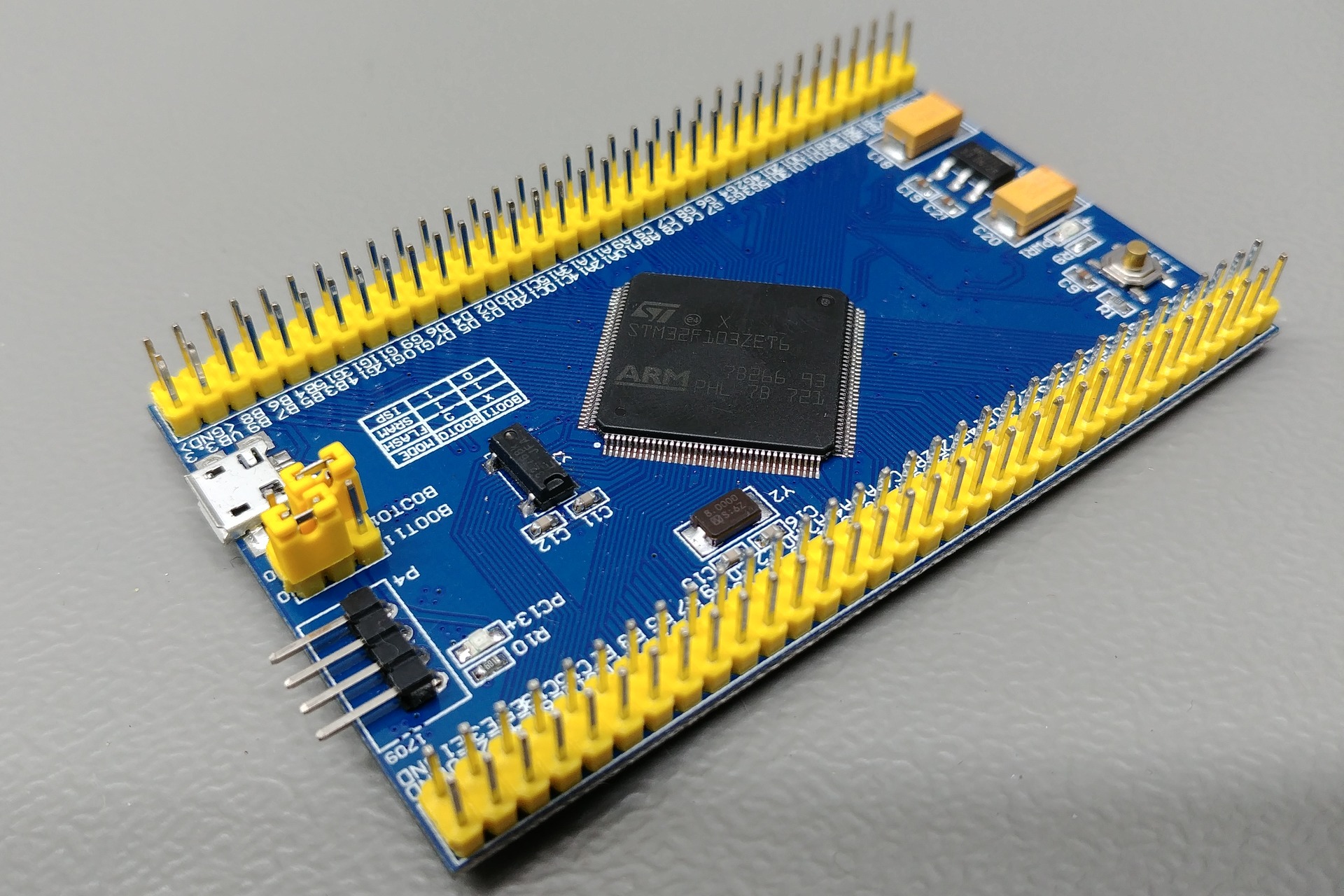
vcc-gnd.com STM32F103ZET6
STM32F103ZET6
Board
| Name | vcc-gnd.com STM32F103ZET6 |
| Part | Unknown |
| Brand | vcc-gnd.com |
| Origin | China |
Microcontroller
| Part | STM32F103ZET6 |
| Manufacturer | ST-Microelectronics |
| Core | Arm Cortex-M3 |
| Max. Clock Speed | 72MHz |
| Package | LQFP 144 pins |
Internal memories
| FLASH | 512KiB |
| SRAM | 64KiB |
Oscillators
| HSI | 8MHz |
| LSI | 40kHz |
| HSE | 8MHz |
| LSE | 32.768kHz |
Power
| Sources | Any +3.3V pin (+3.3V) Any +5V pin (+5V) USB connector (+5V) |
| VDDA pin | No |
| VSSA pin | No |
| VREF- pin | No |
| VREF+ pin | No |
| Backup battery | Pin |
Regulator
| Manufacturer | Advanced Monolithic Systems Inc. |
| Part | AMS1117 (AMS1117) |
| Package | SOT223 3 pins |
| Input | +4.6V to +15V |
| Output | +3.3V @ 1A |
| Datasheet | AMS1117.pdf |
PCB
| Color | Blue |
| Size (w x l) | 20.4mm x 33.4mm |
| Mounting | None |
Remarks
- Warning: The +5V pins on this board are directly connected to the +5V pin of the USB connector. There is no protection in place. Do not power this board through USB and an external power supply at the same time.
Pictures
Inputs
Connectors
Inputs & outputs
Reset button
| Name | RESET |
| Reference | - |
| Type | Button |
| Connected to | NRST |
| Mode | Active low |
BOOT0 jumper
| Name | BOOT0 |
| Reference | - |
| Type | 2-way jumper |
| Connected to | BOOT0 |
| Mode | N.A. |
BOOT1 jumper
| Name | BOOT1 |
| Reference | - |
| Type | 2-way jumper |
| Connected to | PB2 |
| Mode | N.A. |
Power LED
| Name | PWR1 |
| Reference | - |
| Type | LED |
| Connected to | +3.3V rail |
| Mode | N.A. |
User LED
| Name | PC13 |
| Reference | - |
| Type | LED |
| Connected to | PC13 |
| Mode | Sink |
Connectors & headers
Header 1 properties
| Name | Unknown |
| Reference | None |
| Type | Pin header (2.54mm, 33x2, male) |
Header 1 pins
| # | Name | Function | Connected to |
|---|---|---|---|
| 1 | 3.3 | - | +3.3V rail |
| 2 | GND | - | Ground plane |
| 3 | VB | - | VBAT |
| 4 | GND | - | Ground plane |
| 5 | B9 | - | PB9 |
| 6 | B8 | - | PB8 |
| 7 | B7 | - | PB7 |
| 8 | B6 | - | PB6 |
| 9 | B5 | - | PB5 |
| 10 | B4 | - | PB4 |
| 11 | B3 | - | PB3 |
| 12 | G15 | - | PG15 |
| 13 | G14 | - | PG14 |
| 14 | G13 | - | PG13 |
| 15 | G12 | - | PG12 |
| 16 | G11 | - | PG11 |
| 17 | G10 | - | PG10 |
| 18 | G9 | - | PG9 |
| 19 | D7 | - | PD7 |
| 20 | D6 | - | PD6 |
| 21 | D5 | - | PD5 |
| 22 | D4 | - | PD4 |
| 23 | D3 | - | PD3 |
| 24 | D2 | - | PD2 |
| 25 | D1 | - | PD1 |
| 26 | D0 | - | PD0 |
| 27 | C12 | - | PC12 |
| 28 | C11 | - | PC11 |
| 29 | C10 | - | PC10 |
| 30 | A15 | - | PA15 |
| 31 | A14 | - | PA14 |
| 32 | A13 | - | PA13 |
| 33 | A12 | - | PA12 |
| 34 | A11 | - | PA11 |
| 35 | A10 | - | PA10 |
| 36 | A9 | - | PA9 |
| 37 | A8 | - | PA8 |
| 38 | C9 | - | PC9 |
| 39 | C8 | - | PC8 |
| 40 | C7 | - | PC7 |
| 41 | C6 | - | PC6 |
| 42 | G8 | - | PG8 |
| 43 | G7 | - | PG7 |
| 44 | G6 | - | PG6 |
| 45 | G5 | - | PG5 |
| 46 | G4 | - | PG4 |
| 47 | G3 | - | PG3 |
| 48 | G2 | - | PG2 |
| 49 | D15 | - | PD15 |
| 50 | D14 | - | PD14 |
| 51 | D13 | - | PD13 |
| 52 | D12 | - | PD12 |
| 53 | D11 | - | PD11 |
| 54 | D10 | - | PD10 |
| 55 | D9 | - | PD9 |
| 56 | D8 | - | PD8 |
| 57 | B15 | - | PB15 |
| 58 | B14 | - | PB14 |
| 59 | B13 | - | PB13 |
| 60 | B12 | - | PB12 |
| 61 | GND | - | Ground plane |
| 62 | GND | - | Ground plane |
| 63 | GND | - | Ground plane |
| 64 | GND | - | Ground plane |
| 65 | 5V | - | +5V rail |
| 66 | GND | - | Ground plane |
Header 2 properties
| Name | Unknown |
| Reference | None |
| Type | Pin header (2.54mm, 33x2, male) |
Header 2 pins
| # | Name | Function | Connected to |
|---|---|---|---|
| 1 | GND | - | Ground plane |
| 2 | GND | - | Ground plane |
| 3 | E0 | - | PE0 |
| 4 | E1 | - | PE1 |
| 5 | E2 | - | PE2 |
| 6 | E3 | - | PE3 |
| 7 | E4 | - | PE4 |
| 8 | E5 | - | PE5 |
| 9 | E6 | - | PE6 |
| 10 | C13 | - | PC13 |
| 11 | C14 | - | PC14 |
| 12 | C15 | - | PC15 |
| 13 | F0 | - | PF0 |
| 14 | F1 | - | PF1 |
| 15 | F2 | - | PF2 |
| 16 | F3 | - | PF3 |
| 17 | F4 | - | PF4 |
| 18 | F5 | - | PF5 |
| 19 | F6 | - | PF6 |
| 20 | F7 | - | PF7 |
| 21 | F8 | - | PF8 |
| 22 | F9 | - | PF9 |
| 23 | F10 | - | PF10 |
| 24 | C0 | - | PC0 |
| 25 | C1 | - | PC1 |
| 26 | C2 | - | PC2 |
| 27 | C3 | - | PC3 |
| 28 | A0 | - | PA0 |
| 29 | A1 | - | PA1 |
| 30 | A2 | - | PA2 |
| 31 | A3 | - | PA3 |
| 32 | A4 | - | PA4 |
| 33 | A5 | - | PA5 |
| 34 | A6 | - | PA6 |
| 35 | A7 | - | PA7 |
| 36 | C4 | - | PC4 |
| 37 | C5 | - | PC5 |
| 38 | B0 | - | PB0 |
| 39 | B1 | - | PB1 |
| 40 | B2 | - | PB2 |
| 41 | F11 | - | PF11 |
| 42 | F12 | - | PF12 |
| 43 | F13 | - | PF13 |
| 44 | F14 | - | PF14 |
| 45 | F15 | - | PF15 |
| 46 | G0 | - | PG0 |
| 47 | G1 | - | PG1 |
| 48 | E7 | - | PE7 |
| 49 | E8 | - | PE8 |
| 50 | E9 | - | PE9 |
| 51 | E10 | - | PE10 |
| 52 | E11 | - | PE11 |
| 53 | E12 | - | PE12 |
| 54 | E13 | - | PE13 |
| 55 | E14 | - | PE14 |
| 56 | E15 | - | PE15 |
| 57 | B10 | - | PB10 |
| 58 | B11 | - | PB11 |
| 59 | GND | - | Ground plane |
| 60 | 3V3 | - | +3.3V rail |
| 61 | GND | - | Ground plane |
| 62 | 3V3 | - | +3.3V rail |
| 63 | GND | - | Ground plane |
| 64 | 3V3 | - | +3.3V rail |
| 65 | GND | - | Ground plane |
| 66 | 3V3 | - | +3.3V rail |
USB connector properties
| Name | Unknown |
| Reference | None |
| Type | USB Micro |
USB connector pins
| # | Name | Function | Connected to |
|---|---|---|---|
| 1 | - | VCC | +5V rail |
| 2 | - | D- | PA11 via 22Ω resistor (R4) |
| 3 | - | D+ | PA12 via 22Ω resistor (R7), pulled up by 4.7kΩ resistor (R8) |
| 4 | - | ID | Ground plane |
| 5 | - | GND | Ground plane |
SWD header properties
| Name | Unknown |
| Reference | P4 |
| Type | Pin header (2.54mm, 4x1, female) |
SWD header pins
| # | Name | Function | Connected to |
|---|---|---|---|
| 1 | GND | GND | Ground plane |
| 2 | SWCLK | SWCLK | PA14 |
| 3 | SWDIO | SWDIO | PA13 |
| 4 | 3.3V | VCC | +3.3V rail |
Devices
AT24C04 properties
| Name | Unknown |
| Reference | U6 |
| Manufacturer | Microchip Technology Inc. |
| Part | AT24C04 |
| Marking | 24C08N |
| Datasheet | AT24C01-02-04-08-16.pdf |
| Package | SOIC 8 pins |
| Description | 1kB I2C EEPROM |
AT24C04 pins
| # | Name | Function | Connected to |
|---|---|---|---|
| 1 | - | A0 | Ground plane |
| 2 | - | A1 | Ground plane |
| 3 | - | A2 | Ground plane |
| 4 | - | GND | Ground plane |
| 5 | - | SDA | PB7, pulled up by 4.7kΩ (R3) |
| 6 | - | SCL | PB6, pulled up by 4.7kΩ (R2) |
| 7 | - | WP | Ground plane |
| 8 | - | VCC | +3.3V rail |
W25X40CL properties
| Name | FLASH |
| Reference | Unknown |
| Manufacturer | Winbond Electronics Corporation |
| Part | W25X40CL |
| Marking | 25X40CL |
| Datasheet | W25X40CL.pdf |
| Package | SOIC 8 pins |
| Description | 512kiB Dual SPI FLASH |
W25X40CL pins
| # | Name | Function | Connected to |
|---|---|---|---|
| 1 | - | /CS | PA15 via 0Ω (R21), pulled up by 10kΩ (R20) |
| 2 | - | DO | PB4 |
| 3 | - | /WP | +3.3V rail |
| 4 | - | GND | Ground plane |
| 5 | - | DI | PB5 |
| 6 | - | CLK | PB3 |
| 7 | - | /HOLD | +3.3V rail |
| 8 | - | VCC | +3.3V rail |
Generic SRAM properties footprint
| Name | Unknown |
| Reference | U7 |
| Manufacturer | Unknown |
| Part | Generic SRAM |
| Marking | Unknown |
| Datasheet | Unavailable |
| Package | TSOP - II 44 pins |
| Description | Generic SRAM |
Generic SRAM pins footprint
| # | Name | Function | Connected to |
|---|---|---|---|
| 1 | - | A0 | PF0 |
| 2 | - | A1 | PF1 |
| 3 | - | A2 | PF2 |
| 4 | - | A3 | PF3 |
| 5 | - | A4 | PF4 |
| 6 | - | CE | PG10 via 0Ω (R11), pulled up by 10kΩ (R22) |
| 7 | - | I/O0 | PD14 |
| 8 | - | I/O1 | PD15 |
| 9 | - | I/O2 | PD0 |
| 10 | - | I/O3 | PD1 |
| 11 | - | VDD | +3.3V rail |
| 12 | - | GND | Ground plane |
| 13 | - | I/O4 | PE7 |
| 14 | - | I/O5 | PE8 |
| 15 | - | I/O6 | PE9 |
| 16 | - | I/O7 | PE10 |
| 17 | - | WE | PD5 |
| 18 | - | A5 | PF5 |
| 19 | - | A6 | PF12 |
| 20 | - | A7 | PF13 |
| 21 | - | A8 | PF14 |
| 22 | - | A9 | PF15 |
| 23 | - | A10 | PG0 |
| 24 | - | A11 | PG1 |
| 25 | - | A12 | PG2 |
| 26 | - | A13 | PG3 |
| 27 | - | A14 | PG4 |
| 28 | - | A18 | PD13 |
| 29 | - | I/O8 | PE11 |
| 30 | - | I/O9 | PE12 |
| 31 | - | I/O10 | PE13 |
| 32 | - | I/O11 | PE14 |
| 33 | - | VDD | +3.3V rail |
| 34 | - | GND | Ground plane |
| 35 | - | I/O12 | PE15 |
| 36 | - | I/O13 | PD8 |
| 37 | - | I/O14 | PD9 |
| 38 | - | I/O15 | PD10 |
| 39 | - | LB | PE0 |
| 40 | - | UB | PE1 |
| 41 | - | OE | PD4 |
| 42 | - | A15 | PG5 |
| 43 | - | A16 | PD11 |
| 44 | - | A17 | PD12 |
Generic NAND FLASH properties footprint
| Name | Unknown |
| Reference | U8 |
| Manufacturer | Unknown |
| Part | Generic NAND FLASH |
| Marking | Unknown |
| Datasheet | Unavailable |
| Package | TSOP - I 48 pins |
| Description | Generic NAND FLASH |
Generic NAND FLASH pins footprint
| # | Name | Function | Connected to |
|---|---|---|---|
| 1 | - | N.C. | N.C. |
| 2 | - | N.C. | N.C. |
| 3 | - | N.C. | N.C. |
| 4 | - | N.C. | N.C. |
| 5 | - | N.C. | N.C. |
| 6 | - | N.C. | Ground plane |
| 7 | - | R/B | PG6 via 0Ω (R24), pulled up by 10kΩ (R23) |
| 8 | - | RE | PD4 |
| 9 | - | CE | PD7 via 0Ω (R18), pulled up by 10kΩ (R17) |
| 10 | - | N.C. | N.C. |
| 11 | - | N.C. | N.C. |
| 12 | - | VCC | +3.3V rail |
| 13 | - | VSS | Ground plane |
| 14 | - | N.C. | N.C. |
| 15 | - | N.C. | N.C. |
| 16 | - | CLE | PD11 |
| 17 | - | ALE | PD12 |
| 18 | - | WE | PD5 |
| 19 | - | WP | Pulled up by 10kΩ (R19) |
| 20 | - | N.C. | N.C. |
| 21 | - | N.C. | N.C. |
| 22 | - | N.C. | N.C. |
| 23 | - | N.C. | N.C. |
| 24 | - | N.C. | N.C. |
| 25 | - | N.C. | N.C. |
| 26 | - | N.C. | N.C. |
| 27 | - | N.C. | N.C. |
| 28 | - | N.C. | N.C. |
| 29 | - | I/O0 | PD14 |
| 30 | - | I/O1 | PD15 |
| 31 | - | I/O2 | PD0 |
| 32 | - | I/O3 | PD1 |
| 33 | - | N.C. | N.C. |
| 34 | - | N.C. | N.C. |
| 35 | - | N.C. | N.C. |
| 36 | - | VSS | Ground plane |
| 37 | - | VCC | +3.3V rail |
| 38 | - | LOCKPRE | N.C. |
| 39 | - | N.C. | N.C. |
| 40 | - | N.C. | N.C. |
| 41 | - | I/O4 | PE7 |
| 42 | - | I/O5 | PE8 |
| 43 | - | I/O6 | PE9 |
| 44 | - | I/O7 | PE10 |
| 45 | - | N.C. | N.C. |
| 46 | - | N.C. | N.C. |
| 47 | - | N.C. | N.C. |
| 48 | - | N.C. | N.C. |